
We’ve been in 2019 for a while. Although we've covered one or two smartphones in the last couple of months of the calendar year, the true “2019 flagship” phone season is really only starting now. Samsung’s Galaxy S10 is among the first releases in this new wave of phones, and for many markets it outright is the very first of a brand-new generation.
Samsung mixed things up this year by announcing the Galaxy S10 in San Francisco instead of the usual Mobile World Congress event. Though not unprecedented, the big reason here for the change in venues was to reflect Samsung's close collaboration with US carriers such as Verizon on 5G and other matters. Indeed 5G has been pretty much the buzzword for the last year or more, and the last few months have been especially busy in this regard. To that end, there will be a 5G model of the S10, however with its limited availability it doesn’t have nearly the same mass-market appeal as the new mainstream variants of the Galaxy 10.
As we’re nearing this upcoming transition period in technology, the new Galaxy S10 models have instead needed to double-down on the fundamental aspects of the phones in order to entice consumers who are increasingly holding on to their smartphones for three years or more. Here the introduction of a new screen, powerful hardware, bigger batteries, as well as a brand new triple camera setup gives users quite a number of reasons to upgrade.
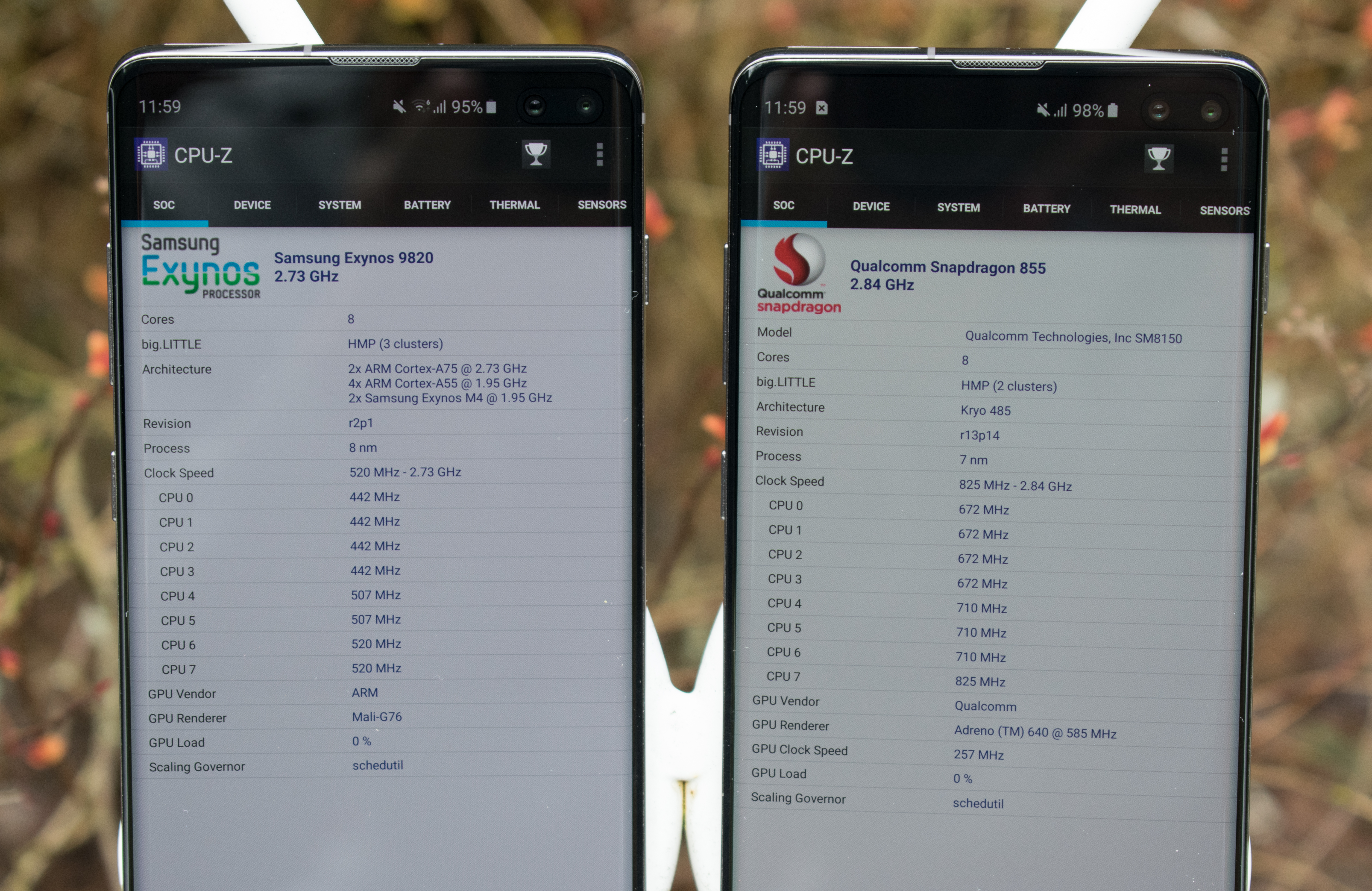
Today we’ll be reviewing the lead member of the Galaxy S10 family, the Galaxy S10+. And in true AnandTech tradition, we're going to look at both variants of Samsung's king of phones: the North American Snapdragon 855 model, as well as the European Exynos 9820 model. With Samsung using different SoCs for what are otherwise (nearly) identical phones, this gives us a unique opportunity to take an in-depth look at the two new processors and compare & contrast them under very similar circumstances. And of course, there's a great deal to dig into with the Galaxy S10’s new screen and triple-module camera setup. This is going to be a long piece so prepare yourselves!
| Samsung Galaxy S10 Series | ||||
| Galaxy S10e | Galaxy S10 |
Galaxy S10+
|
||
| SoC | (North & Latin Americas, China, Japan) Qualcomm Snapdragon 855 Adreno 640 @ 585MHz |
|||
| (Europe & Rest of World) Samsung Exynos 9820 Mali G76MP12 @ 702MHz |
||||
| Display | 5.8-inch 2280 x 1080 (19:9) (flat) |
6.1-inch 3040 x 1440 (19:9) (curved edges) |
6.3-inch 3040 x 1440 (19:9) (curved edges) |
|
| SAMOLED, HDR10+, 1200nits peak brightness | ||||
| Gorilla Glass 5 | Gorilla Glass 6 | |||
| Dimensions | 142.2 x 69.9 x 7.9 mm 150 grams |
149.9 x 70.4 x 7.8 mm 157 grams |
157.6 x 74.1 x 7.8 mm 175 grams (Ceramic: 195g) |
|
| RAM | 6/8GB | 8GB | 8/12GB | |
| NAND | 128/256GB | 128/512GB | 128/512/1024GB | |
| + microSD | ||||
| Battery | 3100mAh (11.93Wh) typ. 3000mAh (11.55Wh) rated |
3400mAh (13.09Wh) typ. 3300mAh (12.71Wh) rated |
4100mAh (15.78Wh) typ. 4000mAh (15.4Wh) rated |
|
| Primary Front Camera |
10MP f/1.9 |
|||
| Secondary Front Camera | - | 8MP, f/2.2 Dual Pixel PDAF "Live focus" |
||
| Primary Rear Camera | 77° Regular Angle 12MP 1.4µm Dual Pixel PDAF Tri-stack CMOS Sensor (Embedded DRAM), 4K60, 1080p240, 720p960 high-speed recording Adjustable aperture f/1.5 or f/2.4, |
|||
| Secondary Rear Camera | 123° Wide Angle 16MP 1.0µm f/2.2 |
|||
| Third Rear Camera |
- | 45° / Telephoto lens 2x zoom 12MP 1.0µm f/2.4, OIS |
||
| 4G Modem | Snapdragon X24 LTE (Snapdragon Integrated) 2G / 3G / 4G LTE (Category 20/13) DL 2000 Mbps (7x20MHz CA, 256-QAM), UL 316 Mbps (2x20MHz CA, 64-QAM) Shannon LTE (Exynos Integrated) |
|||
| 5G Modem | - | |||
| SIM Size | NanoSIM Dual NanoSIM/Hybrid SIM/microSD (Certain models) |
|||
| Wireless | 802.11a/b/g/n/ac/ax 2x2 MU-MIMO, BT 5.0 LE, NFC, GPS/Glonass/Galileo/BDS |
|||
| Connectivity | USB Type-C, 3.5mm headset | |||
| Special Features | Side fingerprint sensor | Under-screen ultrasonic fingerprint sensor | ||
| heart-rate sensor, iris scanner, face unlock, fast charging (Qualcomm QC 2.0, Adaptive Fast Charging, USB-PD), wireless charging & reverse charging (WPC & PMA), IP68 water resistance |
||||
| Launch OS | Android 9.0 with Samsung OneUI | |||
| Launch Prices | 6/128GB: $749/€749/£669 8/256GB: |
128GB: $899/€899/£799 512GB: |
128GB: $999/€999/£899 512GB: 12/1TB: |
|
The big changes of the new Galaxy S10 series can be summed up into three main aspects: a new design with a new screen, new internal hardware with the latest-generation silicon, and a new camera setup consisting of three camera modules.
On the design side, Samsung has continued its tradition of introducing a new design language with every second Galaxy S generation. The S8 and S9 were the first Samsung phones to employ new wide aspect ratio displays, and the new S10 continues this trend towards the inevitable conclusion of a screen-only phone. The key characteristic of the S10+ is the in-display cut-out of the front facing cameras, offering a unique new alternative to the display notch.
The new AMOLED display offers a 3040 x 1440 resolution and now comes with HDR10+ support, with Samsung promising some big increases in peak brightness. We’ll continue on the design of the S10 on the next page in more detail and talk about other new features such as the new under-screen ultrasonic fingerprint sensor.
On the internal hardware side, brand-new SoCs from Qualcomm and Samsung S.LSI promise generational jumps in performance and power efficiency. These latest SoCs benefit from newer manufacturing nodes, upgrades to the CPUs and GPUs, and introducing new dedicated blocks for neural network inferencing in the form of a new DSP and a new NPU.
For the cameras, the Galaxy S10+ incorporates much improved processing as well as support for high dynamic range image capture. And this time around Samsung doesn't include just one or two camera modules, but instead the company has moved up to three rear cameras for their flagship smartphone. Altogether the phone now uses a trifecta of wide angle, regular main, and telephoto modules.
The Galaxy S10 mainline series comes in 3 models: the Galaxy S10e, the regular Galaxy S10, and the up-sized Galaxy S10+. With Samsung offering so many phone variations – 6 in all – we've decided to dedicate our coverage to just a single model. To that end, out of popular demand following last year’s review of the Galaxy S9, we've opted to focus on the headliner Galaxy S10+, taking a look at Samsung's big flagship and the Exynos and Snapdragon versions that it's comprised of.
Hardware Internals
Diving right into the detailed specifications, the SoC situation was quite a controversial topic for Samsung in 2018, with the Samsung LSI (S.LSI) Exynos-powered variant of the Galaxy S9 delivering underwhelming performance and power efficiency compared to its Qualcomm counter-part. And coming into 2019 those concerns are still present as Samsung continues its dual-sourcing strategy.
The challenge for S.LSI (and the new Exynos in particular) is daunting: HiSilicon launched their Kirin 980 SoC nearly six months ago, taking the lead in delivering the first Android SoC built on TSMC’s 7nm manufacturing node. Thanks to its process advantage and Arm’s impressive new Cortex-A76 CPU core, HiSilicon was able to deliver significant performance and power efficiency gains, which we've seen first-hand in devices powered by the new chip. On paper then, the Snapdragon 855 is quite similar to the HiSilicon chip in terms of CPU design and manufacturing technologies, and our first results back in January pointed out to similar great performance and efficiency gains.
We’ll come back to the chipsets in further detail over the next few pages, but suffice it to say, the new chipsets are going to play a critical role in the new phones and will dictate a lot of the user experience of this new generation.
Moving on, let's talk about RAM and storage. The base configurations for the Galaxy S10 and S10+ come with 8GB of LPDDR4X DRAM, while the S10e starts at 6GB, so no phone at any tier is starting short on RAM. What is also great is that Samsung has phased out the 64GB storage tier for this generation, meaning that all S10 models come with at least 128GB of storage. I think this is a pretty important aspect of the value proposition Samsung is making with the Galaxy S10’s base configurations, as it contrasts very favorably against Apple's stingy storage tiers, which sees all of its iPhone configurations start at just 64GB, with the higher-tier 256GB models costing an extra $150.
Going up to higher capacity configurations, the S10e also comes in a 256GB configuration that includes an extra 2GB of DRAM, all of which tacks another $100 on to the price tag. Meanwhile the S10 and S10+ can jump from 128GB of storage to 512GB for an extra $250. And finally at the top, the S10+ is available in an ultra-premium configuration that sports 12GB of DRAM, 1TB of NAND storage, and a ceramic back, for which Samsung is charging a $600 premium over the base configuration.
Another notable change in internal specifications from generation to generation has been the increased battery capacities. The new Galaxy S10 comes advertised with a new 3400mAh battery while the S10+ claims a 4100mAh unit. I say "advertised" here because Samsung is being a bit misleading with their numbers; for the new phones Samsung’s has shifted from listing the design capacity of the batteries to their typical capacity, which inflates the numbers some.
Sticking with the more traditional design capacity then, the Galaxy S10 and S10+ would be rated for 3300mAh and 4000mAh respectively. Which compared to Samsung's last-generation phones, is still a 10% and 14.2% increase respectively over the Galaxy S9 and S9+. In practice, the nominal capacity (actual usable cycle capacity) for one of my S10+ units shows up as 3891mAh, which as it happens is higher than even the 3747mAh showcased on my Note9.
Along with the capacity changes, Samsung seems to have also changed their battery chemistry or charging behaviour, as the PMIC is now programmed to reduce its charge capacity and voltage at 300 cycles instead of 200 cycles. Similarly, the degradation curve appears to have been delayed, and it now reaches a lower 90% of the battery's design capacity after 700 cycles instead of 300. The degradation curves had been rather consistent for a few generations, so it’s interesting to see such a big change in the S10, and it's something to keep an eye on in the next year or two of usage.
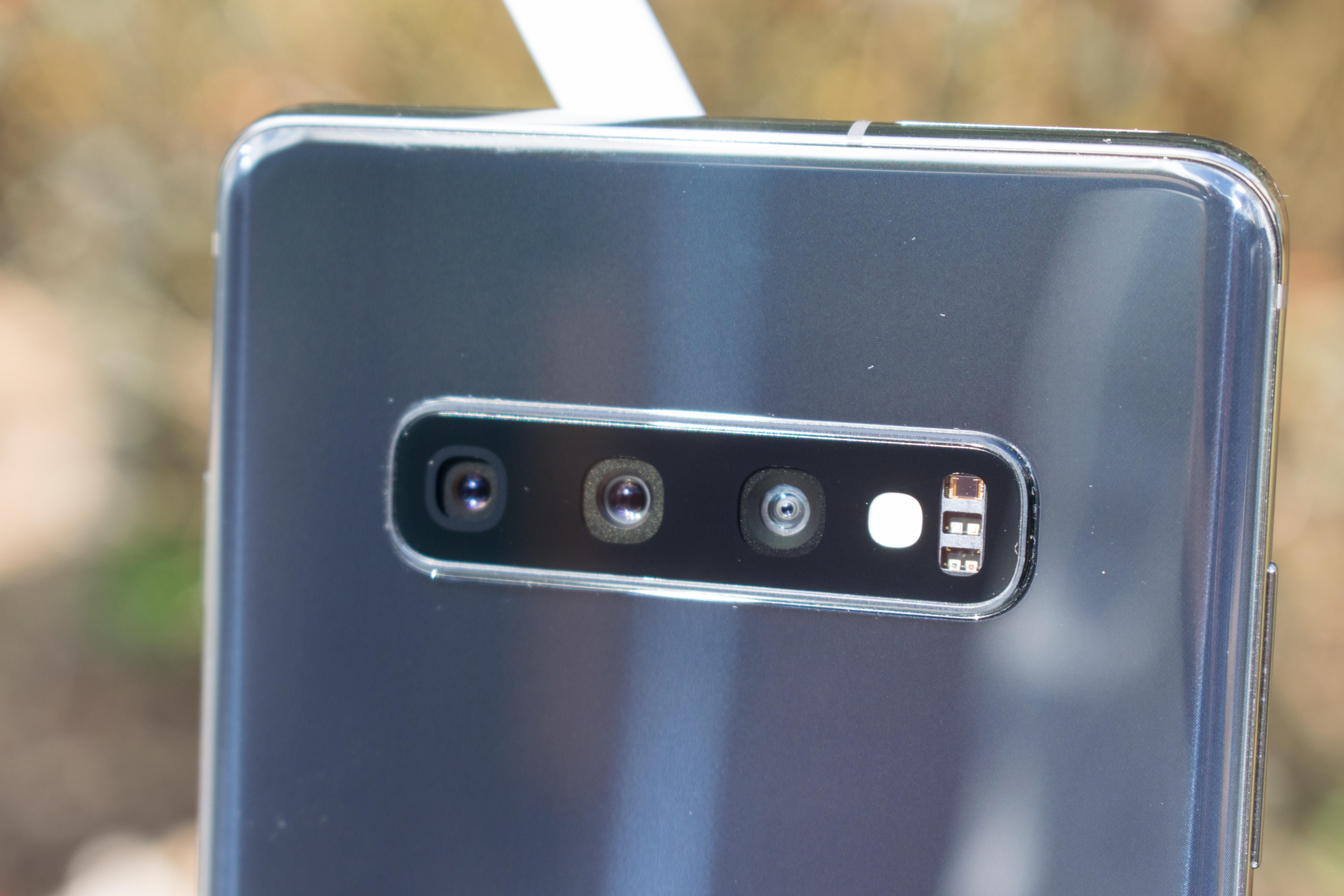
On the back of the phone we have the new horizontal camera layout. The, with the inclusion of three camera modules, the S10 marks the first time Samsung has ever included a wide-angle module in their Galaxy S flagships. After many years of this being an LG-only feature, we suddenly have 3 major vendors all offering a trifecta of regular angle, wide angle and telephoto camera modules.
Relative to the S9, the main and telephoto modules in the S10 haven't changed in terms of their official specifications: they are still 12MP sensors, one with a f/2.4 2x zoom / 45° FoV lens and 1µm pixel pitch sensor, the other with Samsung’s dual-aperture f/1.5 or f/2.4 main module with 77° FoV and a 1.4µm dual pixel PDAF sensor. It’s to be noted that the S10 adopts new sensors for both these modules, even though their specifications on paper remain seemingly the same as on the S9. Added to the duo is the new 16MP f/2.2 1µm pixel pitch 123° wide angle unit, which gives the new Galaxy S10 a new perspective on the world.
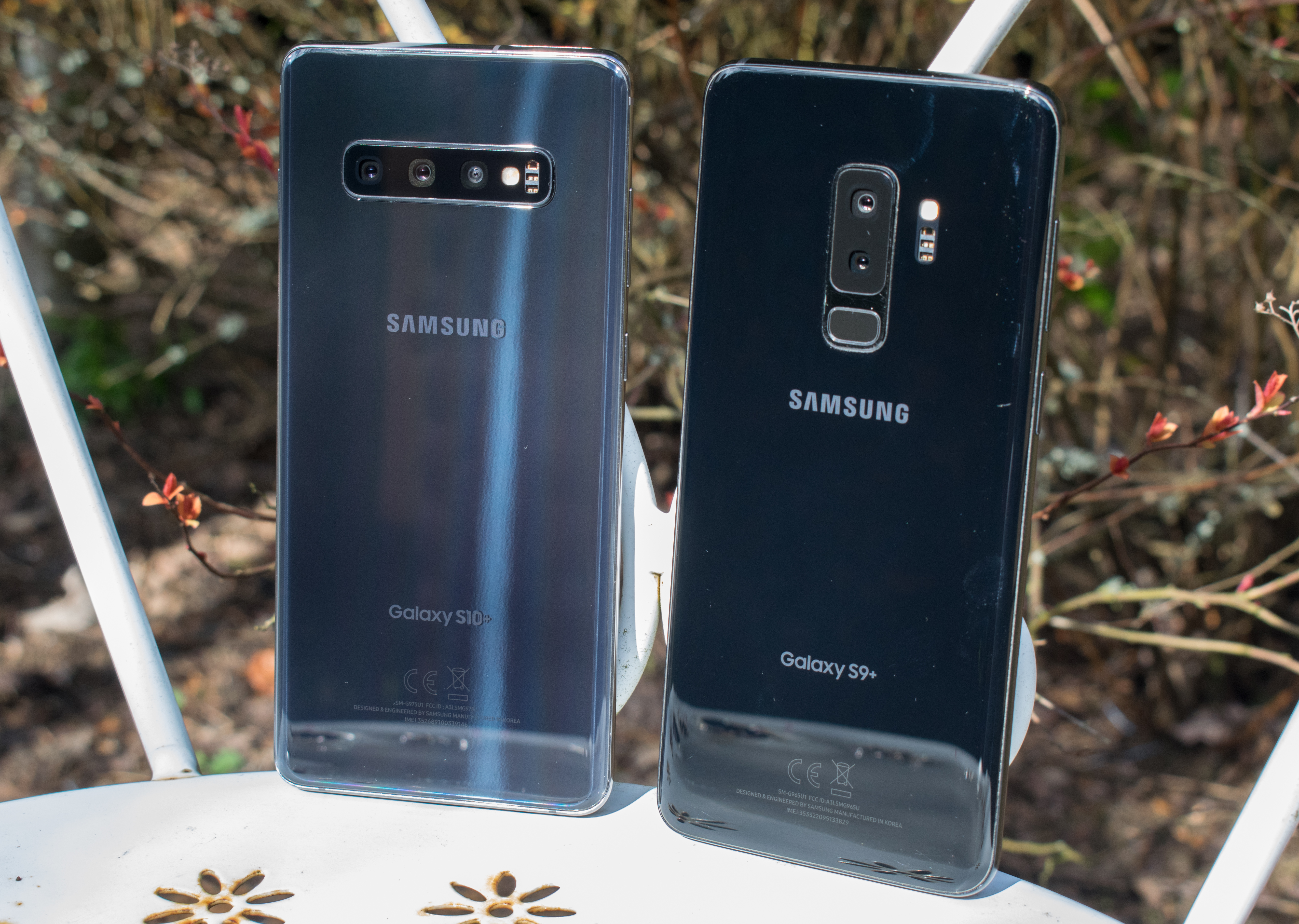
Switching over from internal parts to external features, let’s start with the back of the phone. One interesting thing about the new S10 series right off the bat is their colour scheme. The S10 pictured above is actually the “Prism Black” version, even though it’s glistening in blueish hues. In absence of direct light it does look like a very dark blue, and if there’s any amount of light it has an iridescent sheen to it. Unfortunately it’s still pretty much a fingerprint magnet, and this may be why Samsung chose to sample the Pearl White variants to most media. Personally, I wish Samsung would try out chemically-etched frosted glass finishes, such as those found on the OnePlus 6, LG V40 or Pixel 3, as these are in my opinion the best implementations of glass backs.
Another change of note on the new S10 is that the camera setup has gone horizontal – like on the Note9 – and that the rear fingerprint sensor has disappeared. Qualcomm’s ultrasonic fingerprint sensor has been in the news for a couple of years now, but the S10 is the very first device to actually employ it. The verdict from me is that it's a bit of a mixed bag. The positive thing about the new ultrasonic unit (as opposed to optical units) is that the device doesn’t need to have its screen on to scan your fingerprint. Unfortunately beyond that I’m having a hard time justifying the new sensor compared to other optical implementations.
The core issue here is simply the unlock speed – it’s takes two to three times longer than what the optical sensors on the Mate 20 Pro or OnePlus 6T can achieve. The speed doesn’t seem to be an inherent issue with the sensor itself, as the scanning period isn’t terribly long (still quite slower than an optical sensor), but it takes quite a bit of time for the phone to actually unlock after the fact. Here I have to wonder if the SoC is actually asleep the whole time, and the fingerprint module only wakes it up after having successfully scanned or detected a scan attempt.
It’s to be noted that I tested this with the latest firmware and I didn’t have any issues other reviewers initially described – I can treat it as a usual capacitive or optical sensor, including things like pressing hard and keeping it pressed to unlock. Accuracy has been great and the only instance of failed unlocks has been when I didn’t hold my finger on the sensor for long enough, again coming back to the issue of its slowness. I have to note that I found the Exynos unit to be ever so slightly faster at unlocking, it’s possible that it has newer FP firmware than what's on the Snapdragon unit (US unlocked).
One thing that I very much miss on the Galaxy S10 that I’ve come to love on the S8 and S9 series is the pressure sensitive home button. I wish Samsung at least would mimic the haptics with the fingerprint sensor.
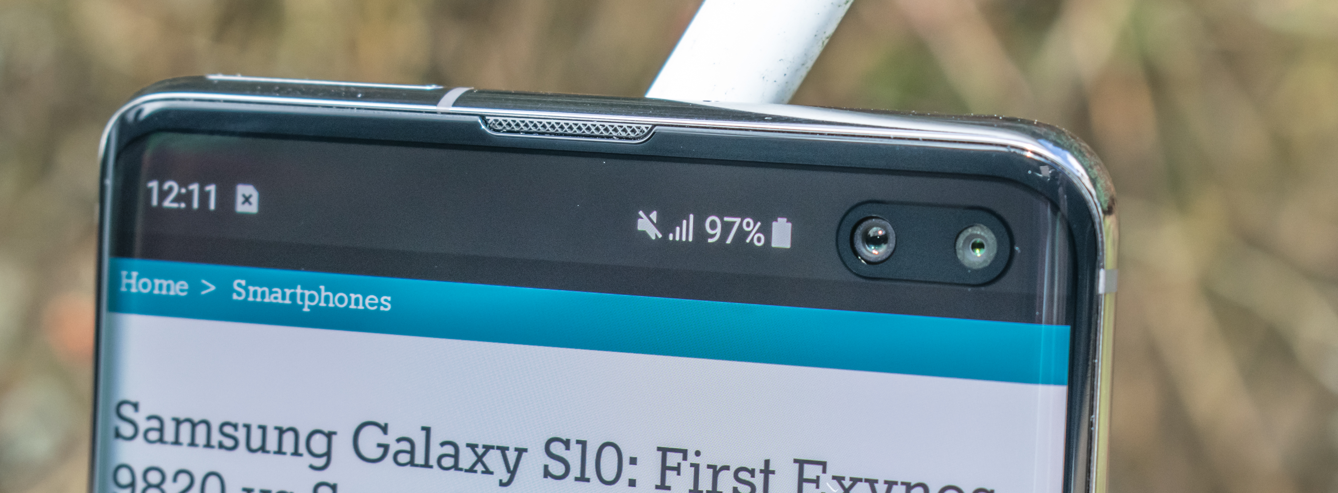
Turning the device to the front, we come to see the Galaxy S10’s most polarising feature: the full-screen display with its camera cut-outs. The new display uses a bigger and wider aspect ratio, now going nearly edge-to-edge, top-to-bottom on the phone. The catch with such designs is that it begs the question of what to do with your usual front sensor and cameras. Samsung last November first talked about the new Infinity displays, and the S10 is an implementation of the Infinity O variant, with a hole-punch cutout.
Now Samsung opted to configure the Galaxy S10+ with two front-facing cameras: one primary module, which is the same as on the regular S10, and one additional optical depth sensor for improved selfie portrait shots. The tradeoff with having two cameras is that you have to choose how to make space for them, either using two holes in the front, or as Samsung chose, a pill-shaped cut-out with both cameras side-by-side. What is actually interesting, and this is visible in sunlight, is that this actually isn’t a pill-shape cut-out at all, but rather two circular cut-outs with a pill-shaped cover just underneath the display glass, above the AMOLED panel. I haven’t seen anybody do a display teardown on the Galaxy S10+ as of yet, but it would be interesting to see if there’s indeed just two holes on the panel with still some sort of covered active area in-between.
The proximity sensor as well as the ambient light sensor have been hidden underneath the screen to the bottom-left of the camera cut-outs. One thing that’s missing from the S10 series – having been dropped by Samsung – is the notification light. Unfortunately at this point in time there’s no substitute for it, and if you aren’t using ambient display notifications, you simply will not see that you have any notifications. Samsung says that this is something that will be addressed in a software update: The plan is that there will be an animation around the camera cut-out serving as a notification light, but this has been delayed for some reason. I also have to wonder what the battery impact of such an implementation would be, as one would have to power on the DDIC just to show such a little light. In any case it is big step backwards in terms of usability and usefulness. I hope the software update addresses this, and that in the future we might have something like a true LED shining from underneath the screen, if it's possible at all.

I’m not particularly a fan of the pill cut-out and haven’t been able to get used to it: Thankfully enabling night mode in the new OneUI settings blacks out the whole top notification area, which drastically reduces how noticeable the cut-out is.

Pitting the Galaxy S10+ against the S9+, we see that the new design hasn’t actually changed the screen real estate much at all at the top of the phone. The bottom of the notification bar ends up at almost the same vertical position on both phones. The vast majority of the notification area is pretty much wasted on the S10+, as its thickness is statically dictated by the camera cut-out. It’s only due to the narrower bottom bezel that we actually get an increase in useable screen-estate for applications.
All of these design tweaks to accommodate the camera cut-out within the UI also means that the area above the camera cut-out doesn't really serve any purpose, as it's not enough space to do anything useful. For that matter, a third of the radius of the cut-out itself is dead area as well, as the camera hole and lens are actually much smaller. The fact that Samsung tries to hide the cut-out in its wallpapers and marketing materials probably doesn't help matters here either – if anything, it makes it look like the company has some level of shame about the feature – so frankly I just don’t see how this offers a better user experience than a notch. Things might look a bit more minimalistic on the S10e and S10, however the issue of vertical space usage remains the same on those variations.
Given all these compromises, one thing seem to be clear, and it corresponds with what I’ve heard towards the middle of last year: Samsung had probably hoped to be able to hide the camera underneath the screen in the initial plans for the S10. However due to technical challenges, they didn’t manage to achieve it for this generation.
In future models, I hope that if Samsung doesn’t achieve a true Infinity display, that at least the hole cut-outs will be smaller and further up near the top bezel of the phone, allowing for better screen real estate usage.

Another very odd design choice for the Galaxy S10s is the new location of the power button. Samsung has shifted this up by a thumb for some reason. This isn’t the first time the button has shifted up, the Galaxy S9 already had moved it up from the S8’s location, but this time the S10 has it in an absurd position.
Usually when I grab a phone I have the bottom right corner dug into my lower palm, and holding it this way it’s simply not possible to reach the power button on the S10+. Instead, I have to readjust how I'm holding the phone just to reach it. This was so annoying for me that I opted to just install Samsung’s One Hand Gesture application, making a gesture just to turn off the screen instead of reaching up to the power button. So far I haven’t heard of any reviewer who hasn’t noticed this big ergonomic regression, and I hope this really is just a one-off design hiccup instead of some conscious design choice by a very long-thumbed Samsung designer. It’s also to be noted that this hardware design goes completely against Samsung’s new OneUI one-handed friendliness.
One thing that I didn’t quite notice during my MWC hands-on is that the S10+ is very much a bigger phone than the S9+. The official dimensions can be a bit deceiving here, as although the S10+ is only 0.5mm wider than the S9+, this measurement is for the outer-edges of the devices. What's not listed is that the Galaxy S10 has a tighter radius on its curved edges than the S9, which make the total circumference of the phone a little longer than its predecessor. In other words, the phone is essentially closer to being squared off at the edges than the S9. This despite the fact that the phone is noticeably 0.4mm thinner.
As a result of these changes, subjectively speaking the S10+ feels like a less ergonomic phone than the S9. Last year I’ve eventually got used to the S9+ over the S9, and I’ll try to see how the S10+ goes for further use. But if was given a choice right now I’d probably opt to change for the smaller S10 due to the ergonomic and power button changes. Again, this is all just my subjective experience, but it’s something that buyers should carefully consider if deciding between the S10 and S10+.
Another big change for the S10 colour options is the fact that Samsung's black variant isn’t actually all black anymore. All colour options now come with a glossy chrome finish frame. Apparently gloss is in vogue, although I prefer a matte finish as it makes for better grip as well as collects less fingerprints.
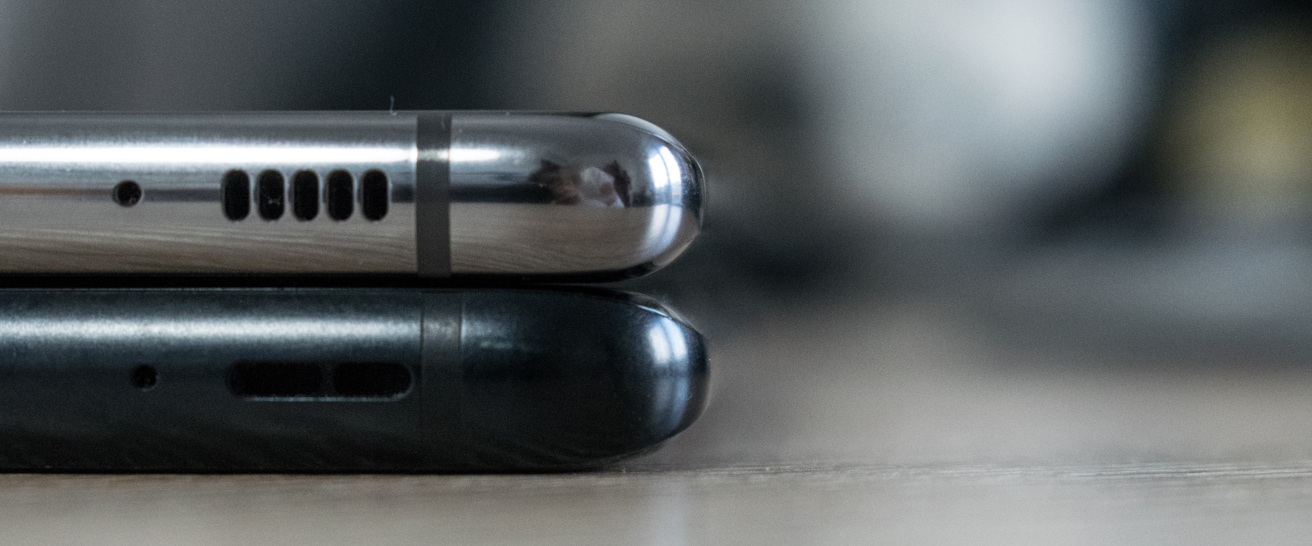
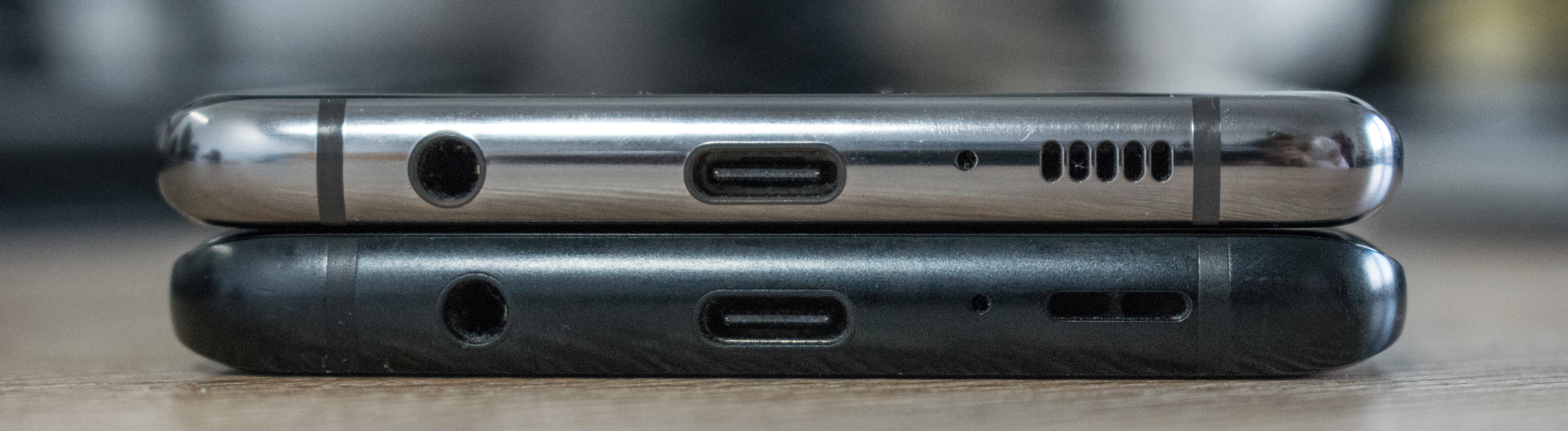
At the bottom of the phone Samsung has reverted to a S8-like grill design for the speaker holes, as opposed to the open slit on the S9. The new speakers on the Galaxy S10 are actually fantastic, and the new earpiece especially shines. I’ll talk more about this in the latter dedicated section.
Lastly, the Galaxy S10 includes a 3.5mm headphone jack. Over the last two years I’ve been very vocal about various manufacturers' irrational desire to remove the jack, and thankfully Samsung is resisting this trend. Instead, Samsung delivers on every single checkbox, including a thin design with a big battery. Though while we're on the subject of audio, it’s to be noted that I again discovered there’s audio discrepancies between the two chipset units this year, something we’ll be addressing a bit later on.
Overall, I think my writing about the Galaxy S10+’s design has been quite critical, more-so than any past Samsung phone. Design aesthetics can be very subjective, so items like the camera cut-out are probably not much of an issue to most people, however I have a much bigger gripe with the S10 when it comes to the ergonomic changes. The one positive change in this regard is that Samsung has managed to noticeably reduce the weight of the phone compared to its predecessors, which helps to make up for some of its other ergonomic changes.
Although the Galaxy S10 is the first Snapdragon 855 device we’re reviewing, Qualcomm’s new chipset shouldn’t come with any major surprises. We had the opportunity to conduct an extensive and in-depth performance preview back in January at CES, which answered a lot of our initial questions about Qualcomm's new flagship SoC. Indeed the Snapdragon 855 largely met our expectations: The new CPU on the new process node performs very similarly to the other 7nm + A76 design we've already seen – the Kirin 980 chipset from HiSilicon – with only minor differences on the CPU complex.
Where Qualcomm strongly differs from the competition is in in the auxiliary accelerator blocks such as GPU, DSP and the new tensor units. Let’s go over the specifications again:
| Qualcomm Snapdragon Flagship SoCs 2018-2019 | |||
| SoC |
Snapdragon 855 |
Snapdragon 845 | |
| CPU | 1x Kryo 485 Gold (A76 derivative) @ 2.84GHz 1x512KB pL2 3x Kryo 485 Gold (A76 derivative) 4x Kryo 485 Silver (A55 derivative) 2MB sL3 @ 1612MHz |
4x Kryo 385 Gold (A75 derivative) @ 2.8GHz 4x256KB pL2 4x Kryo 385 Silver (A55 derivative) 2MB sL3 @ 1478MHz |
|
| GPU | Adreno 640 @ 585MHz | Adreno 630 @ 710MHz | |
| Memory Controller |
4x 16-bit CH @ 2092MHz LPDDR4X 33.4GB/s 3MB system level cache |
4x 16-bit CH @ 1866MHz LPDDR4X 29.9GB/s 3MB system level cache |
|
| ISP/Camera | Dual 14-bit Spectra 380 ISP 1x 48MP or 2x 22MP |
Dual 14-bit Spectra 280 ISP 1x 32MP or 2x 16MP |
|
| Encode/ Decode |
2160p60 10-bit H.265 HDR10, HDR10+, HLG 720p480 |
2160p60 10-bit H.265 720p480 |
|
| Integrated Modem | Snapdragon X24 LTE (Category 20) DL = 2000Mbps UL = 316Mbps |
Snapdragon X20 LTE (Category 18/13) DL = 1200Mbps UL = 150Mbps |
|
| Mfc. Process | TSMC 7nm (N7) |
Samsung 10nm LPP |
|
The Snapdragon 855 is Qualcomm’s first SoC powered by Arm’s new Cortex-A76 CPU core, which we also saw in the Kirin 980. Qualcomm still makes use of Arm’s “Built on Cortex Technology” license, where it requests changes to the CPU IP to be delivered by Arm. The end product ends up marketed as a Kryo CPU – in the case of the Snapdragon 855 the new “Kryo 485” CPU.
In past iterations it’s not always been clear exactly what changes Qualcomm had made to the CPU cores, so it was a surprising and much welcomed change to have the company actually provide concrete examples in the case of the new Snapdragon 855 CPU cores: The two big disclosed changes are an increase of the core’s reorder buffer from 128 entries to a higher, unspecified amount, as well as tuning the prefetchers to better work with floating point workloads.
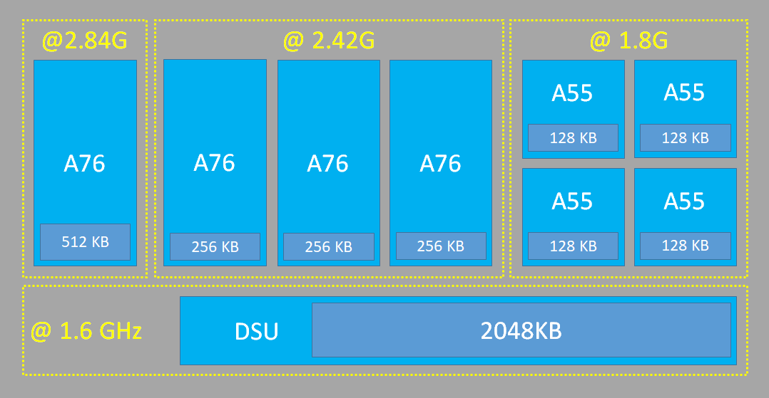
The one thing that makes the Snapdragon 855 unusual though is the new physical CPU configuration. Both the Kirin 980 as well as the Snapdragon 855 both contain four Cortex A76 cores, however the two companies implement these in two completely different ways.
While HiSilicon had opted for a 2+2 core configuration where one pair clocks up to 2.6GHz and the other only reaches 1.92GHz, Qualcomm opts to go with a 1+3 setup. Under Qualcomm's setup one core is clocked up to 2.84GHz, and meanwhile the other three cores reach up to 2.42GHz. While at first glance this makes sense, things get confusing when accounting for the fact that the Snapdragon still only has a single voltage plane for all four CPU cores, whereas the Kirin’s CPU pairs both have their dedicated rails.
Qualcomm has explained that this was a deliberate choice which took into account the actual benefits, as well as (most importantly) the costs of the platform. Having an additional voltage rail means your PMIC needs an additional buck converter and you need to have additional inductors and capacitors on the motherboard, a cost not only in terms of actual component costs but also in terms of valuable PCB space.
What this means is that the power difference between the two CPU groups is much less than one would expect, but most interestingly it will be a difference that is solely dictated by the different physical implementations of the two cores.
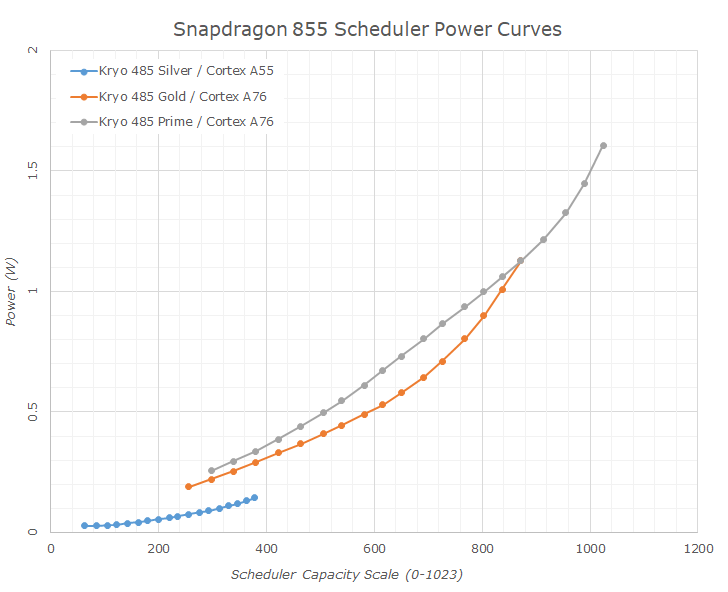
In later sections we’ll address the efficiency difference between the two groups of cores, and one thing that was surprising is that the “middle” cores weren’t that much more efficient than the “prime” core. I extracted the power curves out of the scheduler, as dictated by Qualcomm, and this reveals a bit more information and clarification.
What we see is that the middle “Gold” cores’ power curve shape is shifted down towards lower power, meaning it starts growing at an exponential rate earlier than what we see on the “Prime” core. This would explain why at peak performance, the efficiency difference between the two cores is minor. When we look at the middle frequency points in particular though, we see what this power difference is more notable and actually at its greatest point does represent up to 20% lower power on the mid cores compares to the prime core.
Qualcomm also differentiates the large CPU cores by their cache configuration: The Prime core gets 512KB of L2 while the middle cores make due with 256KB. The Cortex A55’s have the usual 128KB and Qualcomm clocks them conservatively at 1.78GHz.
Finally, the DSU’s L3 cache comes in at 2MB. A big question I had is exactly how fast Qualcomm had clocked the cache at, and the answer is 1.6GHz. This represents a slight increase over the 1478MHz of the L3 cache found in the Snapdragon 845.
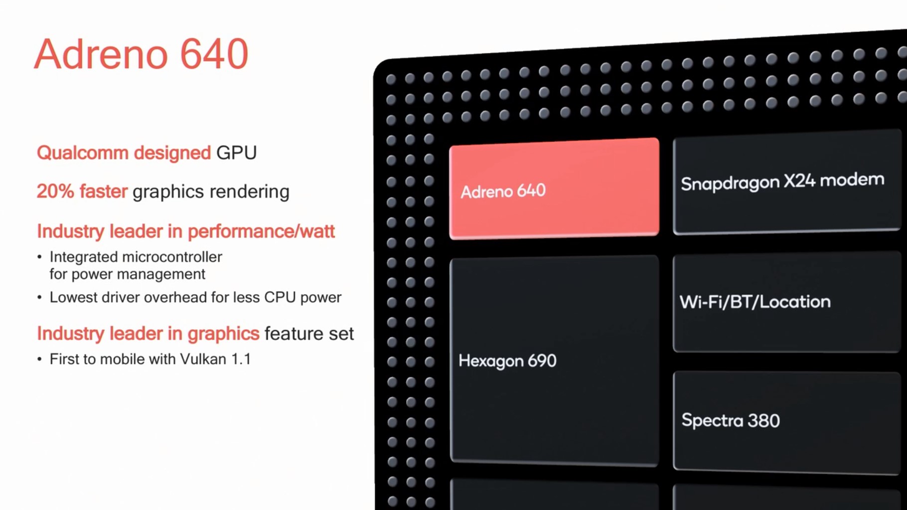
Other large architectural changes in the Snapdragon 855 are the new Adreno 640 GPU. Here Qualcomm supposedly has increased the execution units by 50% - yet only advertise a 20% boost in performance. The explanation here lies in the clock frequency of the new GPU. The Adreno 640 in the Snapdragon 855 runs at only 585MHz, markedly slower than the 710MHz of the Adreno 630. I suspect that Qualcomm saw some of the increasing power usage of the higher clock frequencies and decided it’s better to go wider and slower. Indeed, we’ll see that the Snapdragon 855 has managed to reduce power usage in 3D workloads ever so slightly compared to the Snapdragon 845 – something which should definitely help thermals and sustained performance.
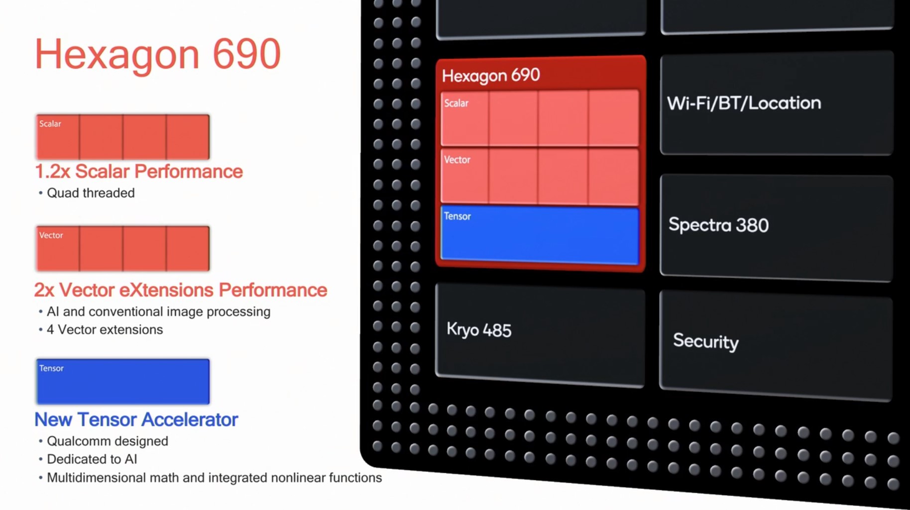
Finally, the new Hexagon 690 DSP block has seen its biggest change in several years. Scalar performance has gone up by 20% through microarchitectural and clock frequency bumps, but most importantly the DSP's vector unit count has been doubled up from two to four units, doubling the HVX performance of the new cores. This is something that will be particularly visible in the AI workloads we’ll cover shortly.
The new tensor accelerator block in the Hexagon IP is a new fixed function unit that is meant to be used for machine inferencing. Currently this unit should likely be exclusively used by Samsung’s first-party software such as the camera app, as Qualcomm won't make it available to NNAPI until later in the year in Android Q. As we’ll see later on, API compatibility and availability these days is going to be a bigger worry than actual hardware performance for these SoCs.
While we know quite a lot about the new Snapdragon 855, information on the new Exynos 9820 has been extremely scarce given S.LSI’s more closed nature. What we know is that the new chip brings with it a new tri-CPU group design and a few vague mentions about its performance and efficiency claims. The chip was announced back in November and I wasn’t too hopeful based on the quoted marketing numbers – the figures needed to be better in order to be able to compete with the Kirin 980 and Snapdragon 855, at least on paper.
Probably the biggest wildcard for the Exynos 9820 is its 8nm LPP manufacturing node. Qualcomm this year had opted to switch over to TSMC’s 7nm manufacturing node for the Snapdragon 855, and the decision looks to be linked to the indisputable superiority of the node.
| Samsung Exynos SoCs Specifications | ||
| SoC |
Exynos 9820 |
Exynos 9810 |
| CPU | 2x M4 @ 2.73 GHz 2x 512KB pL2 2x Cortex A75 @ 2.31 GHz 4x Cortex A55 @ 1.95 GHz Shared complex sL3 @ 4MB |
4x M3 @ 1c2.7 / 2c2.3 / 4c1.8 GHz 4x 512KB pL2 4096KB sL3 4x Cortex A55 @ 1.8 GHz |
| GPU | Mali G76MP12 @ 702MHz | Mali G72MP18 @ 572MHz |
| Memory Controller |
4x 16-bit CH LPDDR4X @ 2093MHz |
4x 16-bit CH LPDDR4X @ 1794MHz |
| ISP | Rear: 22MP Front: 22MP Dual: 16MP+16MP |
Rear: 24MP Front: 24MP Dual: 16MP+16MP |
| Media | 8K30 & 4K150 encode & decode H.265/HEVC, H.264, VP9 |
10bit 4K120 encode & decode H.265/HEVC, H.264, VP9 |
| Integrated Modem | Shannon 5000 Integrated LTE (Category 20/13) DL = 2000 Mbps UL = 316 Mbps |
Shannon 359 Integrated LTE (Category 18/13) DL = 1200 Mbps UL = 200 Mbps |
| Mfc. Process | Samsung 8nm LPP |
Samsung 10nm LPP |
ChipRebel a few weeks ago was able to tear down a Galaxy S10 with the Exynos 9820 and take some great die shot pictures revealing the innards of the new chip.
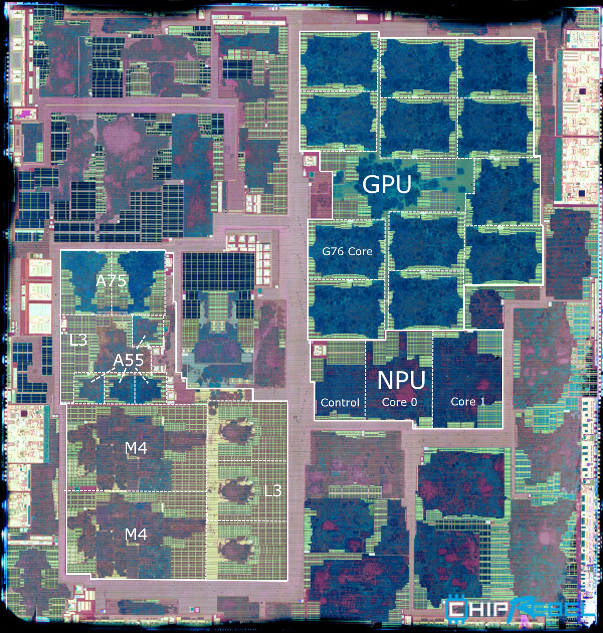
Die shot: Chip Rebel - Annotations/labelling: Andrei @ AnandTech
The one thing that immediately jumps out is the fact that at 127mm², Samsung new chip is extremely large compared to the 73mm² Snapdragon 855. At least in terms of die size, I don’t remember the differences between two SoCs of a generation to have ever been this large.
The new SoC sees the usage of Samsung’s fourth generation CPU core, the M4. The new CPU is codenamed Cheetah, a quite obvious nod to the design team which consists of former AMD folks who were responsible for the big cat line-up of CPU cores.
The CPU cluster is completely re-arranged when compared to last year’s Exynos 9810. A notorious issue with the prior chip was that the little CPU cores weren’t under the same cache hierarchy as the M3 cores, owning to a similar design as found in past SoCs where cache coherency between CPUs was done through the interconnect between them. The new Exynos 9820 now has a similar unified cache hierarchy as found in Arm’s DynamIQ designs, although there are some important differences.
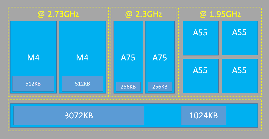
Instead of four big cores, the Exynos 9820 employs only two – the two Cheetah M4 cores clock up to 2.73GHz and are accompanied by two Cortex A75 cores at 2.3GHz and four Cortex A55 cores at 1.95GHz. In fact, the Exynos 9820 is the first tri-CPU cluster/group SoC which actually consists of three different CPU microarchitectures. In practice, the Exynos 9820 is more similar to the Kirin 980 in this regard, just instead of the middles cores being power optimised variants of the big core, it’s just outright a smaller microarchitecture.
Samsung configures the M4 cores with 512KB private L2 caches while the A75’s get 256KB L2’s. Interestingly, Samsung again opted to not configure the A55 cores with L2 caches, instead opting to rely on their custom 1MB L3 slice. It’s here that things become interesting and a bit more exotic than Arm’s DSU. Samsung new L3 cache consists of two different structures. The M4 cores seemingly have access to 3x1MB slices which look to be very similar to the design of the L3 slices found on the Exynos 9810. However on top of this Samsung has a dedicated 1MB slice to which the Cortex A75 and A55 cores have access to. The M4 cores also have access to this 1MB slice, whereas the Cortex don’t have access to the other 3MB of L3.
As of yet I didn't manage to determine how the L3 slices are clocked. On the Exynos 9810 the L3 was on the same clock plane as the big cores, and this might also be the case for the 3MB of the Exynos 9820 as well, but I’m fairly certain the 1MB slice will have a different design and clock plane.
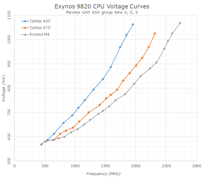
I extracted the voltage tables for my Galaxy S10+ unit which ended up with a mid-tier bin of 5 (Out of usually 13 groups) which is just slightly below what should be the median distribution. Samsung is still extremely aggressive in terms of the peak voltages, going over 1V for all three CPU clusters. The M4 cores went up to 1062mV at 2.73GHz on my unit, and there’s an evident kink in the voltage curve after 2.34GHz where the CPU requires a steep increase in voltage. I didn’t manage to read out the exact voltages on my Snapdragon 855 unit, but it did have a peak voltage on the prime cores at 2.84GHz of 1V, meaning already just by voltage alone the Snapdragon should have an efficiency advantage.
We see similar steep curves on the A75 and in particular the A55 cores. Last year for the Exynos 9820 I argued that it was better to remain on the A55 cores at very high frequencies and high voltages than to power on the M3 cores, but for the Exynos 9820 I have to wonder why Samsung opted to clock the A55 as high, as there’s again a very big efficiency deficit in the top frequencies. If and how this all works out, is going to depend on the scheduler and how it handles transitions between the CPUs.

Looking at Samsung’s scheduler power tables, we see some odd characteristics. According to this, the A75 cores actually aren’t more efficient than the M4 cores, except for at the lower frequencies. What is really irking me however is I can’t seem to understand why the A55 cores are marked to be as high In performance, reaching 42% of the maximum load scale. This characteristic can also be found on the Snapdragon 855. The source code marks that the performance scale is determined by MIPS, which I think is an extremely weird metric to normalise performance with. The reason could be related to how PELT works on the Exynos 9820, however I’ll get back to this topic on the system performance page later in the piece.
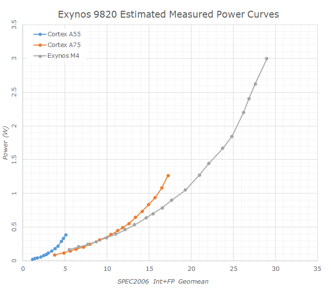
A more real-world power-performance curve would look as above. Here I actually went ahead and measured the SPEC performance and power at their respective peak points and normalised the curves based on this. The Cortex A55 cores in particular see a big down-shift in their relative performance.

Looking at the same data when normalising the x-axis for perf/W instead of absolute power, we again see in more obvious manner that the M4 cores should very much be quite a lot more efficiency than the A75 cores at the same performance, at least for the vast majority of the A75’s upper frequency range. Similarly, the A75’s should be a ton more efficient the A55 cores at the upper performance points of the A55’s. The power figures here consider the active power (load minus idle) of the whole platform, not merely just the CPU cores. This would be a case where race-to-idle at higher power points is actually more efficient than staying on the efficient CPU cores, because of overhead of the rest of the SoC and platform such as memory controllers, DRAM, and PMIC.
It’ll be interesting so see how the Exynos 9820 fares in efficiency, as it has seemingly a large dynamic range in efficiency points.
The GPU on the new SoC is Arm’s new Mali G76 in a 12-core configuration. We had already seen the same GPU in a MP10 configuration employed in HiSilicon’s Kirin 980. In the Exynos implementation, Samsung is clocking the GPU up to at up to 702MHz which is quite higher than the 572MHz of last year’s G72MP18. I’ve noted that the voltages are quite low – 668mV at peak frequency and the voltage curve is quite shallow, meaning efficiency at lower frequencies/performance points won’t be all that much better.
A big new addition this year for Samsung is a new dedicated NPU. The new in-house IP by Samsung is quite intriguing. The company had presented the block as ISSCC this year, revealing some of its high-level workings. The block consists of 3 units: a central control block with a CPU, and two cores which contain the MAC engines. Samsung describes the block as configured in a “butterfly” structure, which specifically addresses in the way the dual-core configuration is set up. In terms of capability, there’s 1024 MAC units and the block runs at up to 933MHz. This means that the raw computational power falls in at 1.86TOPS. However the IP is capable of zero weight pruning, meaning that in real-world quantized models the block can reach a quoted 7TOPS in effective performance. Samsung currently uses the IP in the camera application of the Galaxy S10, using it for scenario recognition for the AI camera feature, always firing up whenever there’s big changes in the viewfinder scene.
Memory is an integral part of a CPU’s performance. We all know that fundamentally memory performance can be summarised into two metrics: The delay it takes to actually access a certain piece of memory, meaning the memory latency, and how much of this memory you can transfer in a given amount of time, meaning the memory throughput, or memory bandwidth. Traditionally, things have been relatively straightforward in terms quantising these metrics, in recent years however, and in particular with this new generation of CPUs, we see things get quite complicated as components such as a CPU’s memory prefetchers can blur the lines between what the physical capabilities of the hardware are and what is actually happening in the real-world.
To better investigate these topics over the last few weeks I’ve invested a bit of time into rewriting our memory test tools from scratch and to attempt to better divulge characteristics of today’s modern CPUs. Unfortunately nowadays publishing a single figure for memory latency isn’t sufficient to properly characterise the memory performance of a platform, and in particular it might not be a valid comparison figure when comparing things between different platforms.
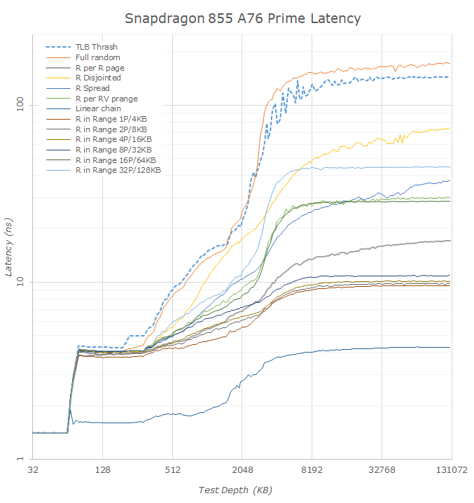
In terms of memory latency tests, the main tools at use are still a variety of pointer-chasing patterns, designed to target different parts of the microarchitectures and bring to light hardware characteristics. In the following page, I can summarize the followings data-points and what they do:
- TLB Trash: This is a simple pattern designed to randomly touch a single cache line per memory page. The goal here is to determine the TLB miss penalty at different TLB levels, and it also exposes the page capacity for each TLB level. Because we’re only touching a single cache line, the actual cache pressure is at an absolute minimum which means for the majority of platforms the actual used memory should fit into L2 caches.
- Full Random: This is a worst case scenario in terms of memory latency. We’re traversing a fully random chain of cache lines throughout the full buffer region. The latency exposed here not only will contain the hardware access latencies, but if the buffer size exceeds the TLB capacity, it will also contain a great amount of TLB miss penalties.
- R per R page: Randomly traverse a random page in the buffer. We also fully randomly access the cache lines within a page, making sure we touch all cache lines before we move on to the next random page.
- R Disjointed, R Spread: Variations of the previous test, but with some permutations in order to attempt to fool some prefetchers.
- R in Range nP/n*pagesizeKB: The memory buffer is dissected into regions of a given size and the regions are randomly traversed. Same principle as R in R page, however at different region sizes.
- R in RV prange: Same as previous, however with non-constant page regions varying from 1 to 32 times page size.
In general, the patterns that matter the most are the TLB Trash, Full Random and for some chipsets the R Disjointed pattern. The latter I mention because I found it to generally be able to fool some of the classical prefetchers. The range patterns are generally caught by most prefetchers nowadays as well, however it’s still interesting to see the results just to have an idea of how aggressive the prefetchers are, and latency curve itself can also reveal different cache latency levels or when one reaches DRAM for certain.
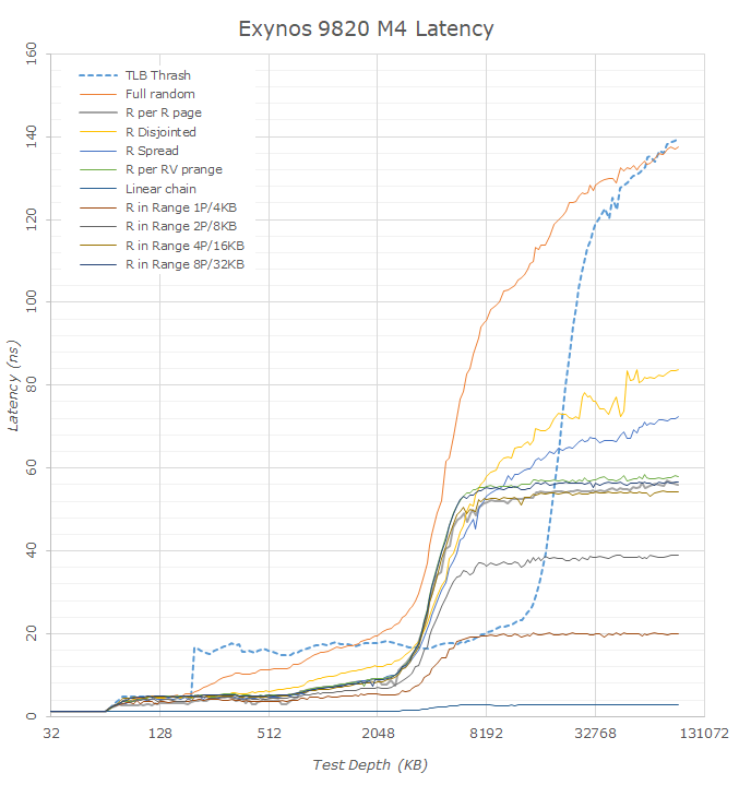
Starting off with the Exynos 9820 on the new M4 cores, we already see a huge difference in the latency behaviour, with the chip showing very different figures than those of the Exynos 9810. To analyse the M4/M3 cores against other microarchitectures we have to keep in mind Samsung’s more unusual TLB hierarchy. The M3 and M4 cores besides the A12’s Vortex cores are the only CPUs whose TLB capacity actually exceeds the equivalent cache hierarchy capacity by a noticeable margin.
Looking at the TLB Trash curve in particular we can see one improvement of the new M4 core is that it upped the size of the microTLB from 32 pages up to 48 pages. Samsung still has an extremely weird behaviour here where if one accesses just a single page more than the capacity of the microTLB then the latency suddenly jumps in a cliff-edge fashion as if the microTLB would no longer be used at all. This is contrasting to the all other CPU cores which have a more gradual transition until the accessed page count is more than double the lowest level TLB capacity, meaning the latency we’re seeing is a gradually raising mix of the lowest level TLB latency plus the next level TLB lookup latency.
As just mentioned, because of the 4096 entry main TLB of the M3/M4, we’re seeing the TLB latency curve go beyond what we actually have in terms of total cache capacity. This has an interesting effect in the full random latency figures of the Exynos 9810 and Exynos 9820 as we have a window between 4MB and ~16MB which in theory contains little to no TLB misses. Looking at the linear and prefetched patterns we see that things flatten out after 7-8MB which signals the end of the effects the cache hierarchy has on the test. Taking this window as an apples-to-apples comparison between the SoCs we see that latencies have gone down from ~124ns on the Exynos 9810 to ~95ns on the Exynos 9820. In theory this latency decrease should be structural to the design of the SoC and its memory controllers, which matches Samsung’s PR about the chip in saying they have made big upgrades in this regard.
Another interesting characteristic we can see is that many of the remaining patterns show drastically lower latency. Instead of showing some kind of structural improvements of the SoC, the actual cause here is the introduction of a new prefetcher on the M4. Here we see the usage of a new spatial memory stream prefetcher which is able to identify higher-level region and depth information in access patterns. Unfortunately for our test tools this means that many of the patterns become useless in terms of determining actual hardware latencies as we can no longer fool the prefetchers.
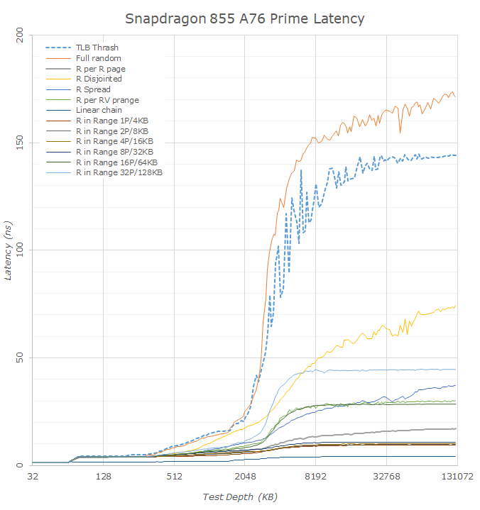
Switching over to the Snapdragon SoCs, we can use a similar methodology to compare the Snapdragon 855 to the Snapdragon 845. It’s to be noted that in terms of the figures here it’s not an apples-to-apples to the Exynos SoC, and the Cortex A75 and A76’s L2 TLB has only 1024 4K page entries, meaning page-table-walk free latency figures are only available till 4MB for the full-random data. Keeping this in mind we can see that the estimated latency from CPU to an active DRAM page is about the same at around 140ns for both SoCs. It’s actually hard to determine the exact figure here as the things vary quite a lot depending what point on the curve we’re measuring. Again, this figure would include page-walk latencies; Qualcomm’s actual structural latency would indeed be much better, around the 90ns figure as shown by some of the patterns on the Snapdragon 845.
What has actually improved drastically in the Snapdragon 855 is the deeper DRAM latency. I didn’t actually go ahead and measure larger test depths, but we can already see there’s a massive difference between the S845 and S855. The former started exceeding 200ns at 128MB while the S855 falls in at 170ns at the same point. Fundamentally this is a structural change in how Qualcomm configures its DRAM architecture in terms of banks and ranks, and greatly improves on some of the bigger latency issues of the Snapdragon 845.
One other thing to note about the new Snapdragon 855 and which also applies to the Kirin 980 is the way the other patterns behave. Arm states that the new Cortex A76 has new state-of-the-art prefetchers and looking at what the CPU is able to do one my patterns I’d very much agree with this claim. Compared to other microarchitectures including Apple’s and Intel’s latest, the Cortex A76 prefetchers are making mince-meat out of my patterns showing the lowest latencies of any platform on the market right now. I tried for a bit trying to design something that would fool the prefetchers but this is something I’ll have to continue working on. The nature of region-based prefetchers means that fundamentally any patterns which has some sort of higher-level repeatability will get caught and predicted, which unfortunately means designing a structured test other than a full random pattern is a bit complicated to achieve.
Switching over from linear graphs to logarithmic graphs this makes transitions in the cache hierarchies easier to analyse.
In the Exynos 9820 M4 results we again see the odd microTLB to mid-TLB behaviour. Interestingly the data would suggest the M4 cores only have access to 3MB of the L3. This would possibly make sense for the Exynos 9820 if the 1MB slice wound be reserved for the A55 and A75 cores. Looking back at the Exynos 9810 data however we see a similar result where the latencies jump at exactly 3MB. That chip didn’t share the L3 with the A55 cores as far as I’m aware, and if Samsung hadn’t confirmed there’s 4MB of L3 on the chip I would have said there was 3MB. I’m not too certain what’s going on here and what happened to that 1MB on the Exynos 9810.
The new A75 cores on the Exynos 9820 very much look like having 256KB L2 caches, and the L3 results points out to being 1MB. What I do find weird is the very long and gradual latency increase the deeper we go into DRAM, as opposed to a more sudden jump. I would attribute this again to how the DRAM banks and ranks are configured on the new chip.
On the Snapdragon 855 we see the 512KB vs 256KB L2 cache difference between Prime and Gold cores. A weird behaviour for which I have no explanation is the latency behaviour between the two cores in the 2-5MB region. Looking at the data, it looks as if the middle cores would have more cache available to them, with the curves being positioned more akin to the behaviour of the Kirin 980 than the Snapdragon 855’s Prime cores. I would have guessed that the Prime cores are bypassing the system level cache/SLC while the Gold cores have access to it, however after having reached out to Qualcomm on the matter they said this was not the case. Thus I remain a bit baffled on what is going on, it's possible this is just measurement noise and there was some activity on the LLC while I testing the Gold cores.
Comparing the L3 curves between the Snapdragon 855 and the Kirin 980 we see the former have better latencies. We don’t know what frequency HiSilicon is running their L3 at, but this lower latency on the part of the Snapdragon could also be due to Qualcomm’s choice of a smaller 2MB cache versus 4MB on the Kirin.
This is also a good opportunity to put Apple’s A12 Vortex core in context. One advantage Apple has in terms of memory architecture is that iOS uses 16KB pages versus 4KB on Android and Windows. While this is a negative for memory allocation space, it’s a positive for performance as there’s less TLB work to be done. Here Apple’s memory hierarchy is quite absurd as it’s just outright flat at excellent latencies till about 3MB, after which some complex TLB behaviour comes into effect.
While memory latency is one part of the story, the other aspect of memory performance is memory bandwidth. In order to test this out I expanded the memory testing tools with tests which also stressed this part of the CPU. The patterns here are quite simple: pure linear bandwidth using SIMD units. In the case of the Arm chips this means 128b NEON instructions while as a comparison data-point the Intel data is using 128b and 256b AVX/AVX2 instructions. The published figures use the STREAM convention, meaning the amount of data that the code explicitly reads and writes.
- ST: pure store bandwidth, we’re just writing static data into memory
- LD: pure load bandwidth, the data here is volatile and we’re merely reading data into registers without doing anything with it
- Flip: Consisting of load and store instructions, within a cache line we flip the words around while flipping the whole data array around on itself on a cache-line basis. Essentially this is exactly the same bandwidth as a memory copy, it’s just that we’re staying within a set memory region.
- CLflip / cache-line flip: We’re flipping the words within cache lines around.
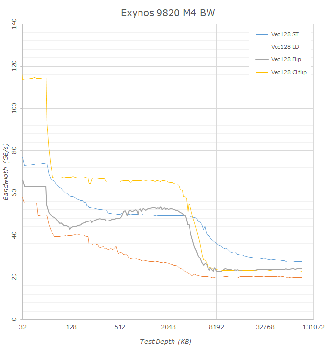
Starting off again with a look at how the new Exynos M4 Cheetah cores compare to last year’s M3 Meerkat, we see that Samsung has significantly improved the bandwidth of the core. Indeed one of the bigger microarchitectural changes of the core was the addition of a second data store unit. To be more precise, one of the prior two load units was converted into a load/store unit, which in theory doubles the store bandwidth of the core. Looking at the data this is confirmed by the L1 store bandwidth which jumps from 36GB/s to 74GB/s. However the improvements look not to be only limited to the store bandwidth as the load bandwidth also increases from 36GB/s to 58GB/s. Memory flip/copy bandwidth on the L1 increases by essentially ~50% from 43GB/s to 66GB/s.
What is odd to see is that flip bandwidth is lower in the L2 cache than it is in the L3, something we also saw in the Exynos 9810. When looking at the different memory bandwidth curves, in particular the store bandwidth of the M3 and M4, we see that in the L3 memory region store curve is actually offset by 1MB compared to the flip/load curves, which ending only after 3MB. That’s bit of an odd thing to explain but reinforces the notion that Samsung is using 1MB of the L3 in a different way. DRAM flip/copy bandwidth increases from 19.5GB/s to 24GB/s which is a little better than the theoretical increase from moving from 1794MHz memory to the 2093MHz used in the new Galaxy S10.
The Snapdragon 855 versus the Snapdragon 845 also sees some big improvements, however the comparison to the A75 might be a bit flawed as the CPU only had a single 128b NEON pipeline and thus it’s possible we’re not really stressing the cache hierarchy at its maximum, with the numbers possibly being lower than what they could be in the L1 and L2 part of the bandwidth curves.
What is really odd to see is the flip/copy behaviour on the new Cortex A76 cores. This zig-zagging pattern also happens on the Kirin 980 and seems to be a characteristic of the microarchitecture, probably some cache-bank access conflict.
The one thing that the Snapdragon 855 differs significantly in compared to the Kirin 980 is the flip/copy bandwidth in the L3 and above, here we see a 50% advantage on the part of the Snapdragon 855 and this continues on into DRAM bandwidth with 21.4GB/s for the Snapdragon versus a meagre 11.7GB/s on the HiSilicon chipset. It’s to be noted that this is indeed near the theoretical bandwidth of the memory controllers at 33.4GB. We’re only measuring 21.4GB/s because this is the STREAM convention bandwidth and not what the hardware is actually doing, in the case of a memory copy the CPU would first read out the contents of the target buffer cacheline before writing into it, meaning the hardware bandwidth would be 50% higher (2 loads 1 store for a memory copy location).
It’s possible to avoid this second memory load when using non-temporal memory stores. Such a mechanism didn’t exist for the ARM ISA prior to ARMv8, but has been around for a while in x86. What is interesting to see is that the new M4 and Cortex A76 pure memory stores essentially behave as non-temporal stores in this test, taking advantage of the ISA’s more relaxed memory model. The store bandwidth in DRAM thus reaches near the theoretical maximum DRAM memory bandwidth with 27.4GB-28GB/s for the Exynos M4 and Cortex A76 in both the Kirin and Snapdragon chipsets. Intel’s 9900K here has to read out the memory location before writing to it, thus only reaches half the theoretical peak of DDR4-3200 at 18GB/s – it’s only with explicit non-temporal store instructions that the Intel core achieves similar behaviour to the new Arm cores. It’s to be noted that Apple’s cores also behave more like Intel’s in this case, showing only 13.9GB/s store bandwidth and also a lower 17.9GB/s flip/copy bandwidth.

The memory bandwidth tests also expose an interesting bottleneck on the part of the Cortex A75 cores inside the Exynos 9820. Here, we see some atrocious performance dip in the L3 memory region. The same test in the Snapdragon 845 with the CPU cores integrated into Arm’s own DSU doesn’t showcase anything anywhere similar to this, so it must be something related to how Samsung has integrated the CPU cores into their own proprietary cluster design. Simultaneous read/writes into the same cache line shouldn’t be all that common in the real-world so it’s unclear exactly how this would impact the CPU’s performance, it does however also show up as a smaller dip in the copy bandwidth of the core.
Memory Level Parallelism
Memory level parallelism (MLP) probably isn’t talked about as much as it should, and we ought to cover the topic more. Last year during the Cortex A76 Tech Day coverage one topic Arm kept mentioning is how its MLP capabilities have massively improved in the new design.
MLP describes multiple accesses to different memory locations, in this context we’re talking about purely single-threaded MLP, meaning a CPU core’s ability to deal with multiple data accesses. If data isn’t located in a CPU’s cache hierarchy it means we have a data miss, however when this happens out-of-order CPUs don’t just merely wait around for the memory access to be fulfilled, but rather go on executing other instructions which aren’t blocked. Exactly how many such data misses the CPU can deal with is called the outstanding miss capability. Traditionally such misses are tracked by miss status holding registers (MSHRs), however I haven’t seen Arm CPUs actually use this nomenclature.
Creating a test for MLP I was inspired by Daniel Lemire’s blog post on the matter and subsequent post on the Apple A12. I integrated a similar concept into my test suite, however took a different approach in regards to the data, adding an extremely important third axis to the data, access depth.
The MLP test here is related to the “Full Random” latency test on the previous page, meaning we’re dealing a chain of random pointers. The difference here is that I’m distributing at equal node distance multiple starting points within the test chain, and traversing it in parallel, scaling up with access pointers (MLP depth).
What is important to note here is that we’re looking just at one aspect of MLP, this being combined core TLB and cache outstanding miss capacity. The data presented is the normalised speedup versus the single-access latency of the full random chain. The Y axis is the speedup factor, while the stacked lines represent the results of the incrementing parallel accesses.
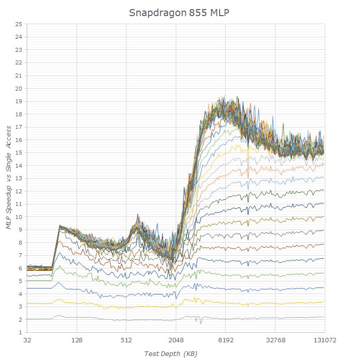
Looking at the Snapdragon 855 first, we indeed see some massive improvements in MLP capability on the part of the Cortex A76 cores, in particular when compared to the prior generation A75 cores. I was actually extremely surprised to see the A75 fare so badly, especially in the L2 region, as the core seemingly is only able to deal with 2-3 outstanding misses. In particular it’s interesting to see that in the L3 region, the A75 cores of the Exynos 9820 fare much better than the same cores in the Snapdragon 845, meaning on the latter chip we might be seeing actual limits in terms of concurrent accesses on the part of the cache.
The new A76 seems to be able to handle 8 outstanding misses to the L2, and we see similar results for of both the Snapdragon 855 as well as Kirin 980. The new core’s MLP capabilities performance on the DRAM side is quite impressive as it seems to handle a peak of 20 outstanding misses and actually sustain 15-16 in deeper memory depths without issues, with also quite linear scaling between MLP depth and actual access speedup.
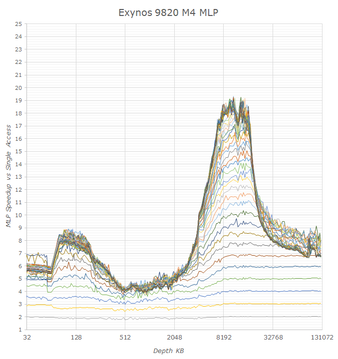
Looking at the Exynos 9820’s performanc, we’re seeing some very big differences to Arm’s newest A76. Indeed even looking back at the Exynos 9810 we see behaviour that reminds us of the TLB issues we saw earlier in the latency analysis: Both the M3 and the new M4’s performance collapses after exceeding the microTLB capacity. Because we’re seeing that on the Exynos 9820’s A75 cores that the L3 cache seemingly is able to handle ~12 outstanding requests, the M3’s and M4’s inability to handle more than 5-6 misses in this regions must be inherently tied to a lack of parallelism on the part of the TLB units on Samsung’s cores. When looking at DRAM outstanding misses it does look like the core can handle 32 misses, however once we’re out of the L2 TLB capacity this again quickly collapses to 7-8 requests. This discrepancy between Samsung’s cores and the new Cortex A76 in the deeper DRAM regions would mean that the actual hardware page table walker on Arm’s cores is able to service double the amount of requests.
It’s also interesting to see how other CPU cores perform in this test. Apple’s A12 Vortex seems to be the outright leader in terms of handling outstanding requests, able to fulfill ~21 requests to the L2 cache and ~41 to DRAM. What is weird is that the A12's speedup scaling is that it isn’t as clean and linear as other cores, and in particular there’s a very weird performance jump from 20 to 21 and 40 to 41 requests which I haven’t found a convincing explanation for yet. It’s also interesting to see what appears to be the last level TLB of the Vortex cores at 2048 pages / 128MB capacity.
On the part of the desktop cores Intel is doing well at ~12 outstanding misses to L2 and 20 to L3, although it can only sustain ~16 which looks to be the TLB limitation. We don’t have the graphs published in this piece but AMD’s Zen does the best in the lower cache hierarchies with a rock steady 16 outstanding misses to L2 and ~30-32 misses to L3 with a 22x speedup and sustaining ~20 to DRAM with a 14-16x speedup.
Overall the Snapdragon and Cortex A76 look to perform extremely well in the MLP aspect and the core does look to bring big improvements in this regard compared to previous generation Arm cores. With this test we’re also exposing some of Samsung’s CPU core bottlenecks – in particular the TLBs seem to be problematic as we’re seeing both latency as well and parallel access limitations that aren’t as pronounced in other cores. The weird memory bandwidth behaviour on the Cortex A75 cores in the Exynos 9820 also points out that the custom design has some rough edges that hopefully would be sorted out in future generations.
Having shed a bit of light on the new microarchitectural aspects of the memory subsystems of the new Snapdragon 855 and Exynos 9820, the question is now how the new chipsets perform in more significant macro workloads. For a continued reference CPU workload we’re again falling back to using SPEC.
The SPEC harness we’re using is compiled with simple and straightforward “-Ofast” compilation flag with the Android devices having an instruction tuning to Cortex-A53s as I’ve found this to give the highest average scores across a the wide range of SoCs.
It’s to be noted that SPEC2006 has been deprecated in favour of SPEC2017, however as the 2006 variant is well understood in terms of its workload characterisation for this article I’m still sticking the older version. We’ll be switching over to SPEC2017 later this spring/summer and covering any new data in a separate article.
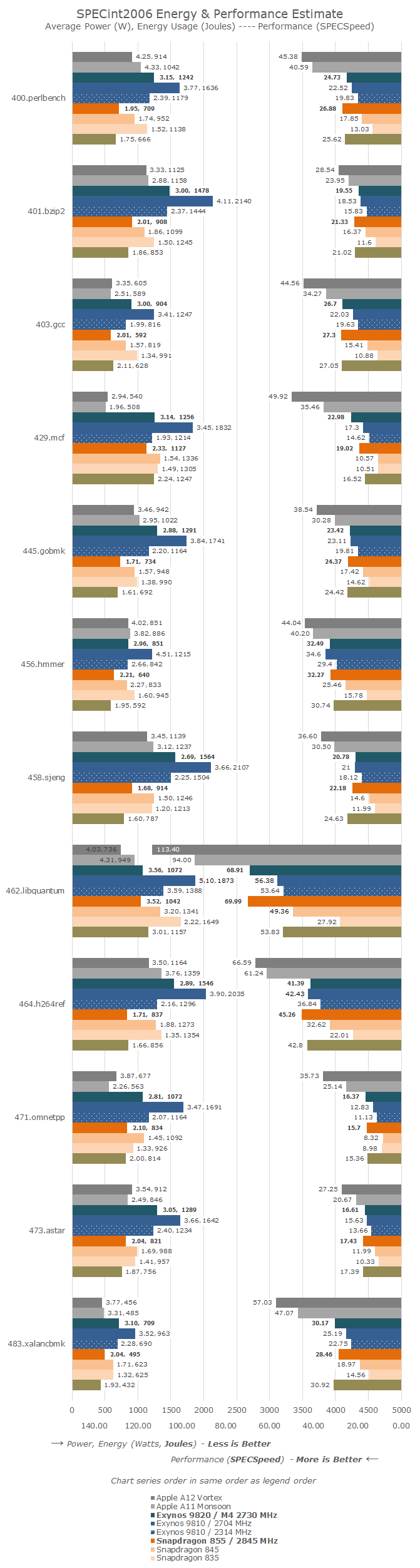
In the SPECint2006 suite of integer workloads, both chipsets don’t showcase any big surprises in performance. The new Snapdragon 855 variant of the Galaxy S10+ confirms the performance figures we were able to measure on the QRD platform back in January with little to no deviation. The Snapdragon posted excellent performance improvements over the Snapdragon 845 of last year and ties in with the Kirin 980 as the fastest Android SoCs for this year.
The Exynos 9820’s performance figures are also relatively unsurprising for me as I had muted expectations. Here we do see some relatively healthy performance improvements considering that we’re talking about mostly IPC gains on the part of the new Cheetah cores, as the new chipset is a mere 30MHz faster than last year’s chip.
The biggest improvements are found in 429.mcf as well as 471.omnetpp where the new M4 cores perform respectively 32% and 27% better. Both these workloads are the most latency and memory sensitive workloads in the SPECint2006 suite, so given the new chip’s improved memory subsystem it’s no wonder that it’s here where we see the biggest performance jumps. Mcf is also one of the rare tests where the Exynos manages to beat the Cortex A76’s in the S855 and K980 by a more significant amount. Unfortunately for the rest of the workloads being tied is the best-case scenario as it loses out by a small amount in all other workloads.
One thing that I have to note is that it’s possible that big parts of the benchmark probably weren’t run at the peak 2.73GHz clocks of the new M4 cores. Samsung has now enabled a current limiter circuit on the CPU cores and will now more aggressively throttle down the frequency of the CPU in high-power workloads. This means that needy workloads will only see the peak frequencies in the range of 5-10 seconds before throttling down to frequencies of 2.3-2.5GHz. I didn’t have time to have a more thorough monitoring of what the chip is doing during SPEC so it’s something I’ll have to follow up on.
When it comes to power efficiency, the new Exynos 9820 does improve notably compared to last year’s Exynos 9810. It seems that the biggest power efficiency improvements happened on the most memory intensive workloads, in particular 462.libquantum’s 74% efficiency improvement all while improving performance is quite impressive.
Having said that, as I had theorized back based on Samsung’s own marketing numbers, the efficiency gains just aren’t enough to actually compete against the 7nm Cortex A76 cores in the new Snapdragon and Kirin chipsets as Samsung’s chip loses out in every workload.
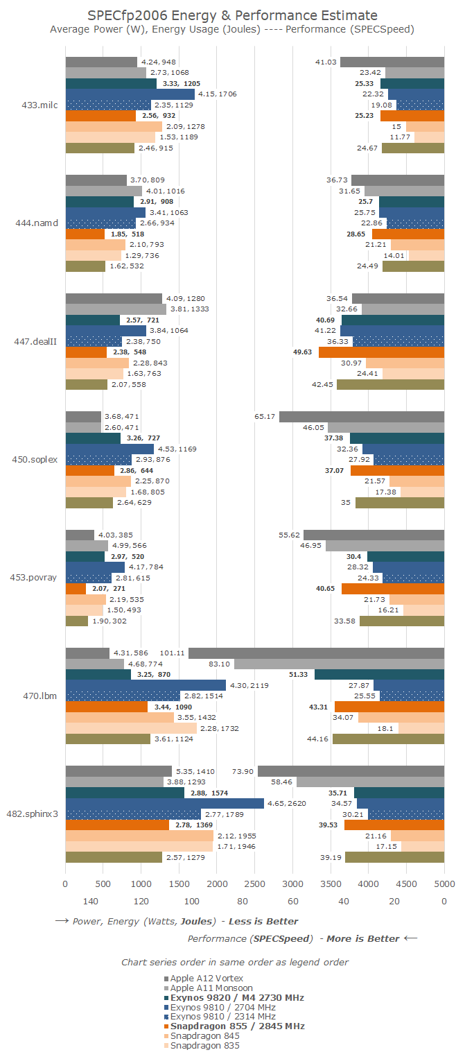
In the C/C++ workloads of SPECfp2006 we see a similar picture as in the integer workloads. The Snapdragon 855 distinguishes itself here as being able to distance itself more from the Kirin 980 in a few workloads such as 447.dealII and 453.povray, all while maintaining almost equal excellent power efficiency.
The Exynos 9820 here has a hard time showcasing big performance improvements compared to its predecessor, but the one workload where we see a massive jump is 470.lbm, with an 84% jump in performance compared to the M3 cores of last year. This workload is particularly latency and bandwidth intensive so the new load/store unit arrangement of the M4 cores seem to favour it a lot.
In terms of power efficiency, what is interesting is that the new Exynos doesn’t lose as badly as in some of the integer workloads, although it still very much loses to the Snapdragon and Kirin.
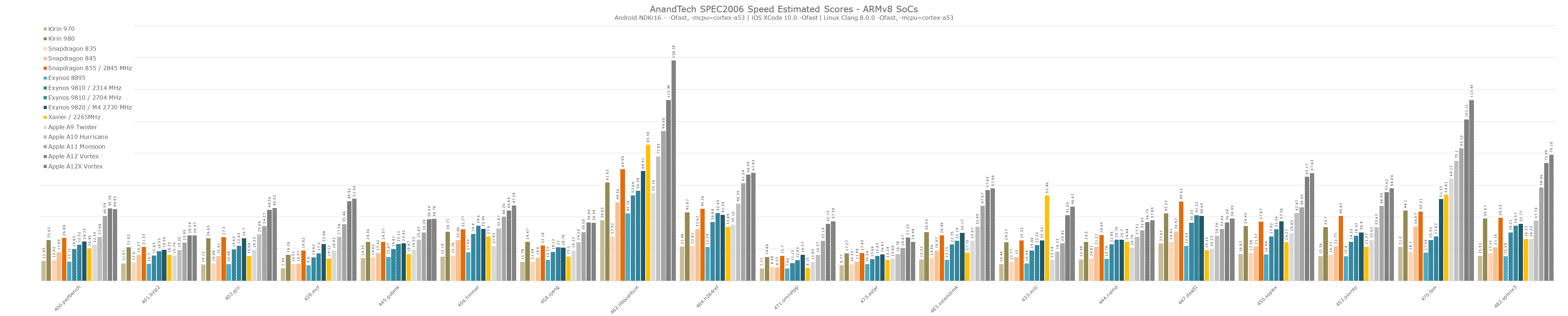
Again to have a wider range of performance comparison across ARMv8 cores in mobile here’s a grand overview of the most relevant SoCs we’ve tested:
Finally it’s important to have a wider overview of the performance and efficiency of the current generation chipsets:

In the SPECint2006 geomean score, the Exynos 9820 slightly loses out in the to the Snapdragon 855. More importantly, it uses 47% more energy and power to achieve this same performance. In SPECfp2006 this efficiency difference drops to 21% - although the performance on the M4 cores is also 7% less.
What is most interesting about the new Snapdragon 855 and Exynos 9820 chips is that they have multiple CPU groups, so I went ahead and also measured performance and power of the middle Cortex A76 cores of the Qualcomm chipset against the Cortex A75 cores of the Samsung silicon.
Unexpectedly, the Snapdragon chipset’s “middle” cores beat the Exynos’ middle cores by a hefty amount. At 2.4GHz, the three middle cores of the Snapdragon actually aren’t weak by any means, and only fall behind the Prime core by 15-19% in performance, for an 18% frequency deficit. The Cortex A75 cores on the Exynos chip are 35% weaker than the middle cores of the Snapdragon. Here a more even comparison probably would have been the 1.92GHz middle A76 cores of the Kirin 980, however I wasn’t able to benchmark them separately on Huawei’s devices.
Energy efficiency of Samsung’s A75 cores are good – although it comes at a larger performance deficit, they’re in line with the energy consumption of the A76 cores in the competition.
In the quest to find an answer on how much the actual process node impacts power efficiency between the 7nm Snapdragon and 8nm Exynos, I also went ahead and ran SPEC on the Cortex A55 cores of both chipsets. After a gruelling 11.5 hours of runtime we finally see that the little cores only post a fraction of the performance of the big core siblings. What is actually quite embarrassing though is that the power efficiency is also quite atrocious for the given performance. Here other blocks of the SoC as well as other active components are using up power without actually providing enough performance to compensate for it. This is a case of the system running at a performance point below the crossover threshold where racing to idle would have made more sense for energy.
Apple’s small cores are just such an incredible contrast here: Even though the absolute power isn’t that much bigger than the Cortex A55 cores, the Tempest and Mistral cores are 2.5x faster than an A55, which also results in energy efficiency that is around 2x better.
Finally getting back to the reason why I measured the A55 cores: The Exynos 9820 here again loses out not only in performance but also in power efficiency. Even though the chip’s A55 cores are clocked in higher at 1.95GHz, it’s likely the lack of L2 caches is handicapping the CPUs in IPC, and thus falls behind the 1.78GHz Snapdragon A55’s. Power efficiency here is better on the Snapdragon SoC by 15-18%.
During last summer’s Hot Chips presentation of the M3 CPU core Samsung had remarked to me that the M4 would be the competing against the Cortex A76, and not the M3. While in terms of power efficiency there’s the matter of us not having a valid apples-to-apples process node comparison at hands, at least from a performance perspective it doesn’t look like the new M4 cores are all that impressive, as they just barely manage hold up against the A76 in the Snapdragon and Kirin. Samsung’s CPU just looks to still have too many rough edges and bottlenecks, and thus ends up performing far below of what we’d expect of a microarchitecture that fundamentally on paper is wider than Arm’s Cortex A76.
Having covered the new CPU complexes of both new Exynos and Snapdragon SoCs, up next is the new generation neural processing engines in each chip.
The Snapdragon 855 brings big performance improvements to the table thanks to a doubling of the HVX units inside the Hexagon 690 DSP. The HVX units in the last two generations of Snapdragon chips were the IP blocks who took the brunt of new integer neural network inferencing work, an area the IP is specifically adept at.
The new tensor accelerator inside of the Hexagon 690 was shown off by Qualcomm at the preview event back in January. Unfortunately one of the issues with the new block is that currently it’s only accessible through Qualcomm’s own SDK tools, and currently doesn’t offer acceleration for NNAPI workloads until later in the year with Android Q.
Looking at a compatibility matrix between what kind of different workloads are able to be accelerated by various hardware block in NNAPI reveals are quite sad state of things:
| NNAPI SoC Block Usage Estimates | |||
| SoC \ Model Type | INT8 | FP16 | FP32 |
| Exynos 9820 | GPU | GPU | GPU |
| Exynos 9810 | GPU? | GPU | CPU |
| Snapdragon 855 | DSP | GPU | GPU |
| Snapdragon 845 | DSP | GPU | GPU |
| Kirin 980 | GPU? | NPU | CPU |
What stands out in particular is Samsung’s new Exynos 9820 chipset. Even though the SoC promises to come with an NPU that on paper is extremely powerful, the software side of things make it as if the block wouldn’t exist. Currently Samsung doesn’t publicly offer even a proprietary SDK for the new NPU, much less NNAPI drivers. I’ve been told that Samsung looks to address this later in the year, but how exactly the Galaxy S10 will profit from new functionality in the future is quite unclear.
For Qualcomm, as the HVX units are integer only, this means only quantised INT8 inference models are able to be accelerated by the block, with FP16 and FP32 acceleration falling back what should be GPU acceleration. It’s to be noted my matrix here could be wrong as we’re dealing with abstraction layers and depending on the model features required the drivers could run models on different IP blocks.
Finally, HiSilicon’s Kirin 980 currently only offers NNAPI acceleration for FP16 models for the NPU, with INT8 and FP32 models falling back to the CPU as the device are seemingly not using Arm’s NNAPI drivers for the Mali GPU, or at least not taking advantage of INT8 acceleration ine the same way Samsung's GPU drivers.
Before we even get to the benchmark figures, it’s clear that the results will be a mess with various SoCs performing quite differently depending on the workload.
For the benchmark, we’re using a brand-new version of Andrey Ignatov’s AI-Benchmark, namely the just released version 3.0. The new version tunes the models as well as introducing a new Pro-Mode that most interestingly now is able to measure sustained throughput inference performance. This latter point is important as we can have very different performance figures between one-shot inferences and back-to-back inferences. In the former case, software and DVFS can vastly overshadow the actual performance capability of the hardware as in many cases we’re dealing with timings in the 10’s or 100’s of milliseconds.
Going forward we’ll be taking advantage of the new benchmark’s flexibility and posting both instantaneous single inference times as well sequential throughput inference times; better showcasing and separating the impact of software and hardware capabilities.
There’s a lot of data here, so for the sake of brevity I’ll simply put up all the results up and we’ll go over the general analysis at the end:
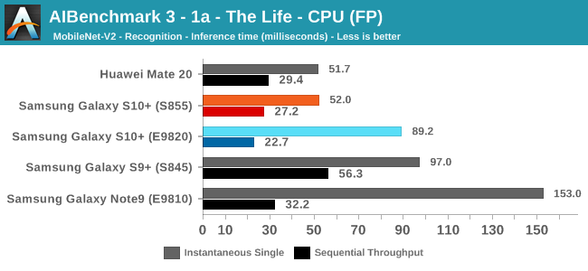
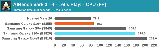
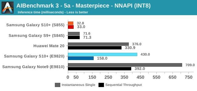
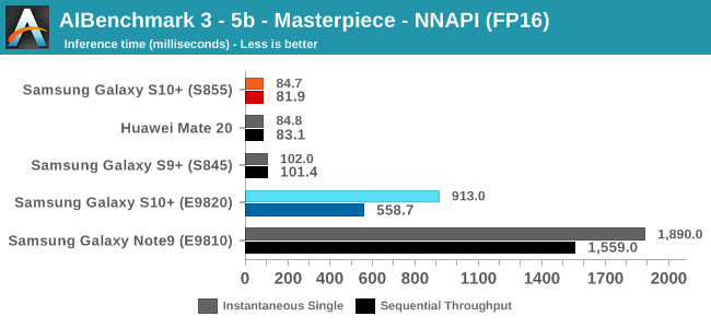
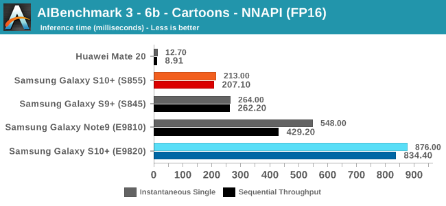
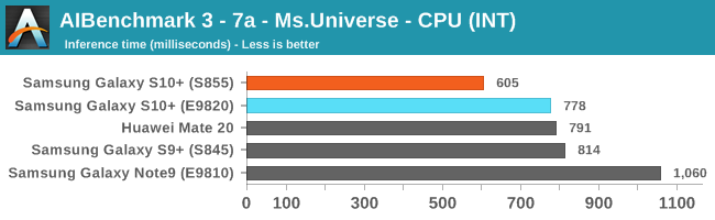
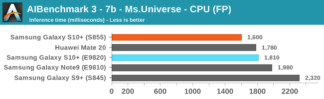
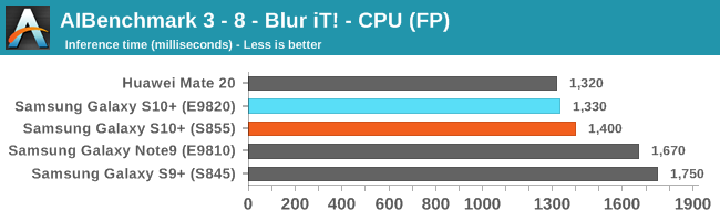
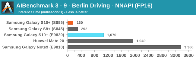
As initially predicted, the results are extremely spread across all the SoCs.
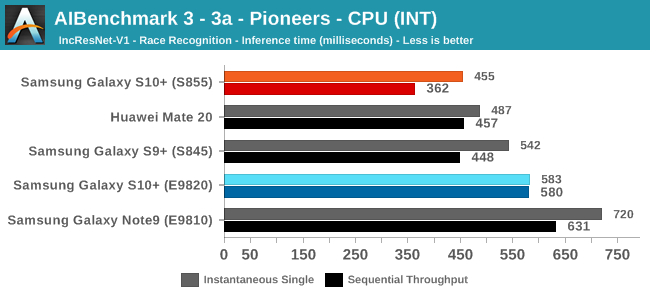
The new tests also include workloads that are solely using TensorFlow libraries on the CPU, so the results not only showcase NNAPI accelerator offloading but can also serve as a CPU benchmark.
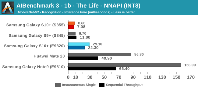
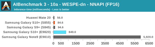
In the CPU-only tests, we see the Snapdragon 855 and Exynos 9820 being in the lead, however there’s a notable difference between the two when it comes to their instantaneous vs sequential performance. The Snapdragon 855 is able to post significantly better single inference figures than the Exynos, although the latter catches up in longer duration workloads. Inherently this is a software characteristic difference between the two chips as although Samsung has improved scheduler responsiveness in the new chip, it still lags behind the Qualcomm variant.
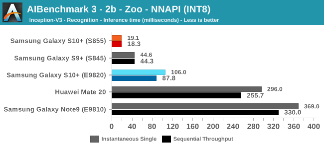
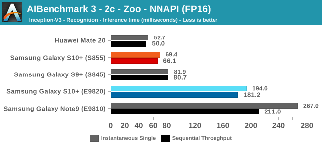
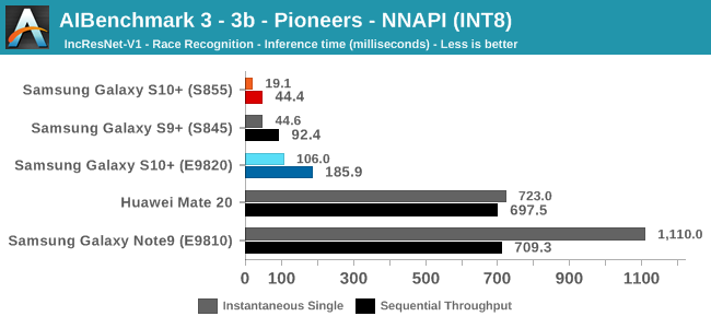
In INT8 workloads there is no contest as Qualcomm is far ahead of the competition in NNAPI benchmarks simply due to the fact that they’re the only vendor being able to offload this to an actual accelerator. Samsung’s Exynos 9820 performance here actually has also drastically improved thanks to the new Mali G76’s new INT8 dot-product instructions. It’s odd that the same GPU in the Kirin 980 doesn’t show the same improvements, which could be due to not up-to-date Arm GPU NNAPI drives on the Mate 20.
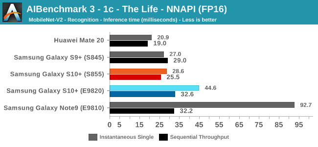
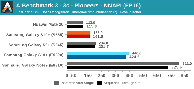
The FP16 performance crown many times goes to the Kirin 980 NPU, but in some workloads it seems as if they fall back to the GPU, and in those cases Qualcomm’s GPU clearly has the lead.
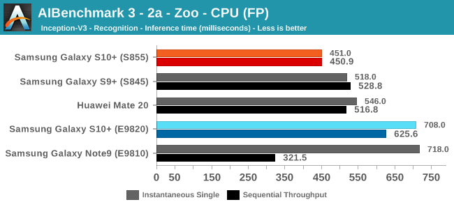
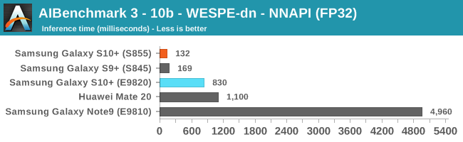
Finally for FP32 workloads it’s again the Qualcomm GPU which takes an undisputed lead in performance.
Overall, machine inferencing performance today is an absolute mess. In all the chaos though Qualcomm seems to be the only SoC supplier that is able to deliver consistently good performance, and its software stack is clearly the best. Things will evolve over the coming months, and it will be interesting to see what Samsung will be able to achieve in regards to their custom SDK and NNAPI for the Exynos NPU, but much like Huawei’s Kirin NPU it’s all just marketing until we actually see the software deliver on the hardware capabilities, something which may take longer than the actual first year active lifespan of the new hardware.
As we’ve extensively covered in various over the last year and more, CPU performance alone doesn’t signify all that much if the system isn’t able to properly take advantage of it in order to achieve better user experience.
Software here plays and incredibly important role, and we’ve seen some devices fall face flat in this regard. Last year’s Exynos 9810 powered Galaxy devices in particular made it abundantly clear just how much of a user experience difference this can make, vastly overshadowing the actual hardware performance.
For the Galaxy S10, we expand on our initial MWC coverage regarding system performance between the two chipset variants. Here we saw clear indications that the Snapdragon 855 variant would again win in these set of benchmarks, and likely end up as the better device in terms of user experienced performance.
We’ve retested the numbers with our own in-house devices, so let’s take a look if and how things have changed:
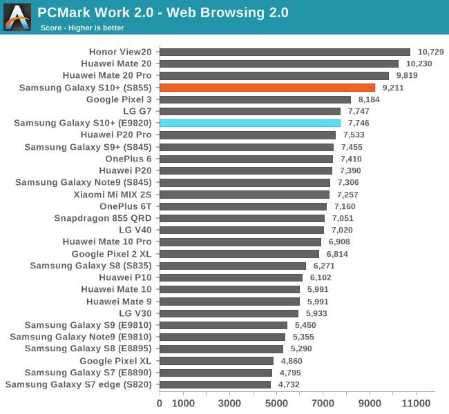
Starting off with the PCMark web-browsing workloads, the Snapdragon 855 variant of the Galaxy S10 leads the benchmark scores. Even though we’re seeing the Qualcomm chipset in a production device now, it still looks to lose out to the Kirin 980 devices. Both Samsung and Huawei now have “performance” modes in the device settings. For Huawei, as per company product management explanations, this is actually the intended full performance of the device while the default mode is slightly more battery friendly for the mass-market users who aren’t as performance sensitive.
It’s not yet exactly clear what Samsung’s performance mode changes compared to the “optimised” default setting, however I’ve also seen that this latter setting can result in throttled performance which actually results in Snapdragon performance numbers falling back to the range of the Exynos 9820 figures.
Samsung’s new “CPU Limiter” for the Galaxy S10 now works fundamentally differently than last year; it doesn’t actually limit the peak frequency the CPU can reach, but rather limits the total CPU capacity to 70% in the scheduler, meaning multi-threaded workloads will be throttled. Frankly I find this silly as the device doesn’t inherently become more efficient as it still has access to the higher frequencies, and thus the battery advantage of this function isn’t nearly as great as what users will have experienced with the Galaxy S9.
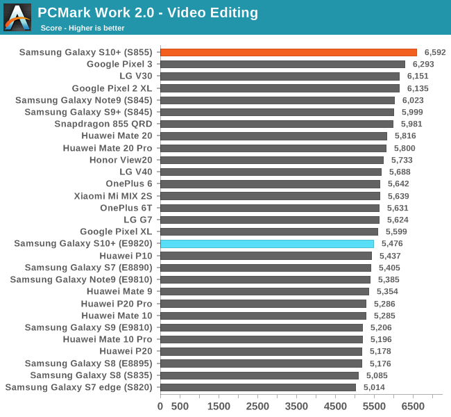
The video editing workload is still something dominated by Qualcomm. The performance here seems to be dictated by the responsiveness of the little cores. In absolute terms, the differences aren’t big and this part of PCMark isn’t very indicative of overall system performance.
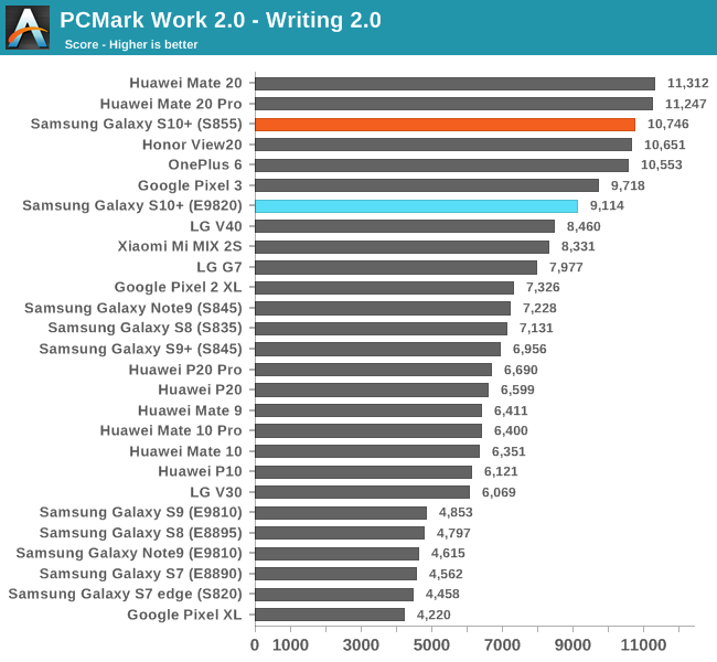
The one test that is actually most indicative of experienced device responsiveness is the Writing 2.0 workloads. Here the Snapdragon 855 falls in at the top of the performance charts along the Kirin 980. The Exynos 9820 Galaxy S10 also does relatively well here, but just falls short of the competition.
What is however most important is that this is now the first Exynos chipset in several years where S.LSI was able to deliver a scheduler and DVFS system that wasn’t absolutely abysmal, as evidenced by the massive performance difference between the Galaxy S10 and past Exynos devices at the very bottom of the chart.
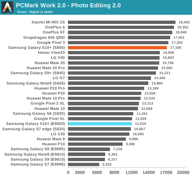
The Photo Editing workload again showcases similar improvements on the part of the Exynos. Here Qualcomm still has a very large performance advantage which simply might be due to better GPU acceleration for the RenderScript workloads which are part of the photo filter editing in this test.
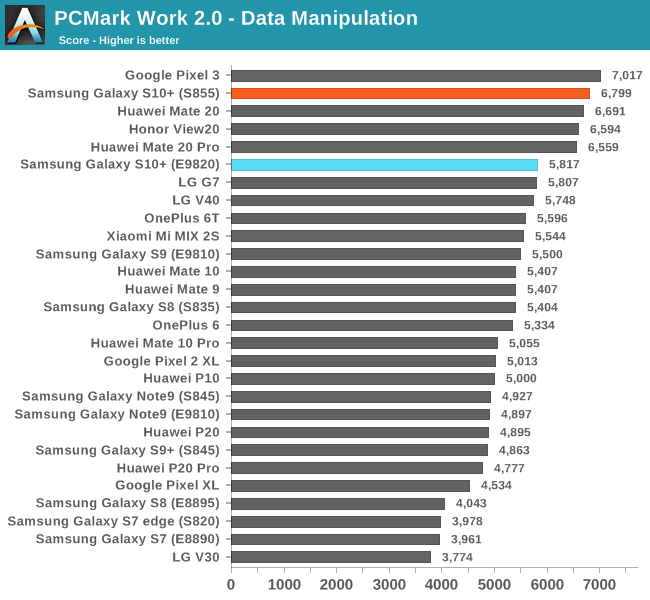
Finally the Data manipulation workload sees the Snapdragon Galaxy S10 again at the top of the charts, with the Exynos 9820 slightly trailing it.
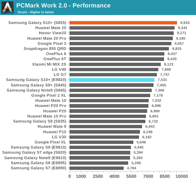
Overall, the Snapdragon 855 Galaxy S10 ends up as our top performing phone in PCMark. The Exynos 9820 unit trails behind, however does showcase significant improvements over previous generation Exynos phones.
Web JS Benchmarks
Switching over to web-browser based benchmarks, we’re testing inside a simple OS WebView shell as this is most representative of user-experience when browsing websites through third-party apps.
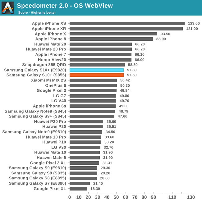
In Speedometer 2.0, both Galaxy S10 devices are neck-in-neck within margins of error. The performance improvements of the Snapdragon 855 over last year’s Snapdragon 845 in this test seems relatively conservative, the Kirin 980 clearly is able to showcase a bigger performance lead.
The Exynos 9820 showcases dramatic performance gains over last year’s Exynos 9810. The removal of the abysmal hot-plugging mechanism means that the big CPU cores are able to actually run at full speed all while having secondary threads on the other big and middle cores.
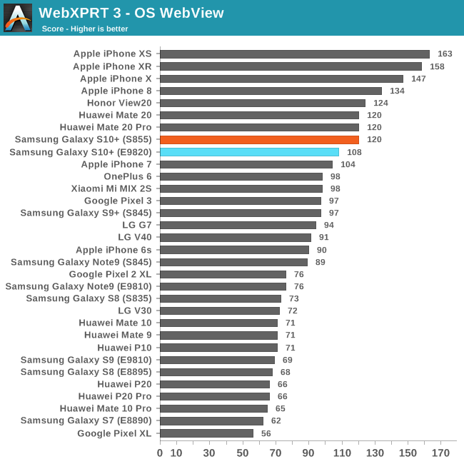
In WebXPRT 3, the Snapdragon 855 manages to match the Kirin 980 while Exynos 9820 trails slightly behind.
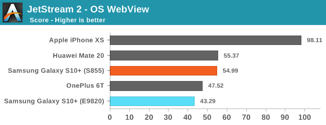
Finally, I wanted to add in results of the brand-new JetStream 2 test that was released just two days ago and we’ll likely looking to adopt in the future (after more careful analysis). An interesting aspect of this test is that it’s using web workers to parallel workloads, something we usually never had in the past for browser-based JavaScript benchmarks.
Here the Exynos 9820 has a bigger disadvantage than the Snapdragon 855. The fact that the Kirin 980 scores identical to the Snapdragon means the performance shouldn’t be linked to the lower performance middle cores, but still strongly dependent on the big core performance. Unfortunately this seems to be another benchmark that doesn’t agree with Samsung’s CPU microarchitecture, with the Exynos S10 falling behind by 22%, even scoring less than the Snapdragon 845 of last year. This workload also doesn’t seem like a constant sustained test so it’s likely that scheduler responsiveness will play a role.
Scheduler & DVFS responsiveness
To investigate scheduler responsiveness and device DVFS settings, we fall back to your scaling performance ramp test. This is a fixed instruction chain workload with fine-grained timing collection every certain amount of instructions. By converting the time taken for every instruction block we can convert this into the frequency of the resident CPU that the workload is currently scheduled on, giving us detailed frequency information over time.
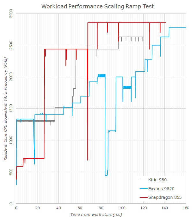
We’re looking at both Galaxy S10 units as well as the Mate 20 with the Kirin 980. For the new Qualcomm chipset what stands out is that the Galaxy S10 is indeed more aggressive in its scaling than what we’ve seen in January on the Qualcomm reference platform, reaching peak performance in 67ms rather than 95ms. It’s interesting that now even though the Qualcomm chipset has a clear scheduler and DVFS speed advantage over the Kirin 980, it still only is able to match or slightly lose out to the HiSilicon chip.
The results of the Exynos 9820 aren’t nearly as performant as on the Snapdragon Galaxy S10. Here we’re seeing that the chip first scales and resides on the small A55 cores for up to 83ms before it switches over to the Cortex A75 cores. What is extremely weird here is that the workload is staying on the middle cores for a mere 15ms before it switches over to the big M4 cores, finally reaching peak performance at around the 143ms mark, essentially twice as slow as the Snapdragon chipset.
We’ve seen a similar story last year with the Exynos 9810, and the issue is inherently tied to the scheduler. Make no mistake here, the Exynos 9820 behaves infinitely better than the Exynos 9810, however I expected more of the new chip. One of the things I did last year was to introduce two new big changes to the scheduler’s load tracking mechanism; halving the PELT half-life from 32ms down to 16ms which by itself doubled the responsiveness. On top of that I’ve added util_est to increase performance of short periodic workloads that otherwise would have lost their load utilisation faster.
For the Exynos 9820, what Samsung did was essentially also adopt these two important changes… and that’s about it. Although the new chipset comes with a new scheduler that does make efforts to schedule things around in an energy efficient way, the core issue of the scheduler load being slow hasn’t been further improved beyond what I myself was able to achieve last year. Currently the Exynos 9820 is the only flagship Android SoC that still uses PELT in its scheduler as a load tracking mechanism as both Qualcomm and HiSilicon are making use of WALT, which is massively more responsive. Google actually wants to drop WALT out of the Android Common Kernel, however this happened only after PELT was made to be as responsive as WALT. One very important patch to achieve this is unfortunately missing from the Exynos 9820’s BSP which means as a delivered product the Exynos Galaxy S10 just has lower responsiveness. In next year’s Exynos we’ll probably finally see things equal out, however this will by then be 4 generation and years of Qualcomm SoCs being superior and giving better user experience simply because they have the better software stack.
That being said, it’s not all doom and gloom for the new Exynos 9820 Galaxy S10. What the scheduler lacks is actually made up by touch boosting as well as Android framework integrated boosters which are triggered by activity switches. These mechanisms actually help out a lot the user experience of the Exynos Galaxy S10 beyond what we can actually measure in standalone benchmarks such as PCMark or the web tests. In my subjective experience with both phones, yes the Snapdragon unit was slightly faster, but if I didn’t have both devices side by side to compare, it would be have been something quite hard to notice. What is important is that the experience on the Exynos 9820 is leagues ahead of what we’ve seen in the Exynos 9810 devices and past chipsets. Some of these OS-side boosters seem to have made it into the Android P update of Exynos 9810 devices, so while the kernel as remained largely unchanged, at least this part benefits last year’s devices.
Overall, both the Snapdragon 855 and Exynos 9820 Galaxy S10 give among the very best performance experiences among current Android phones, even if the latter has some rough edges here and there.
On the GPU side of things, Qualcomm has long been leading the benchmark charts with the help of their in-house Adreno GPU architecture. With the Galaxy S10, we again see a new round of Adreno vs Mali in the Snapdragon and Exynos variants of the phone.
The Adreno 640 in the Snapdragon 855 has relatively conservative performance targets this generation. Here Qualcomm promises 20% better performance even though the GPU itself has a reported 50% more execution units. What has happened is that Qualcomm has dropped the clock frequency from 710MHz down to 585MHz, account for where most of that theoretical GPU performance is missing. The rationale here is to be able to run wider and slower, and thus more efficiently.
On the Exynos side of things, the new chip adopts a new Mali G76MP12 GPU clocked in at up to 702MHz. We’re already seen the GPU inside of the Kirin 980, however for whatever reason Samsung S.LSI has always been able to achieve better results than HiSilicon for several generations in a row, so it’ll be interesting to see how these two chipsets differ.
Starting off with the 3Dmark Sling Shot Extreme Unlimited test suite, the Physics workload is mostly a CPU bound test within a GPU thermally constrained scenario.
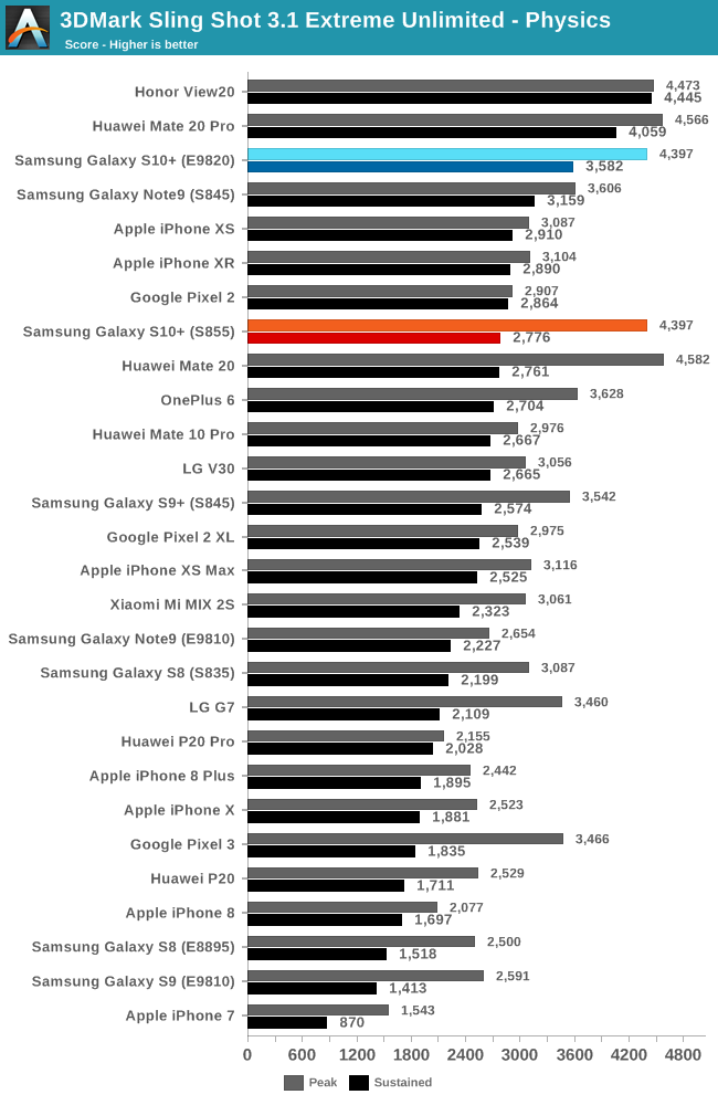
The Exynos 9820 surprisingly takes the performance lead between both Galaxy S10 units. The result here is a very big change compared to previous generation Exynos SoCs. I hadn’t had the time to investigate if this is actually caused by improvements of the new M4 core or if the workload is being scheduled on the A75 cores. Both peak performance and sustained performance here are very good and are only beaten by Kirin 980 devices.
The Snapdragon 855 Galaxy S10 also posts excellent peak perf results, however the CPU seem to throttle quite a bit more, falling in line with what last year’s Snapdragon 845 devices were scoring.
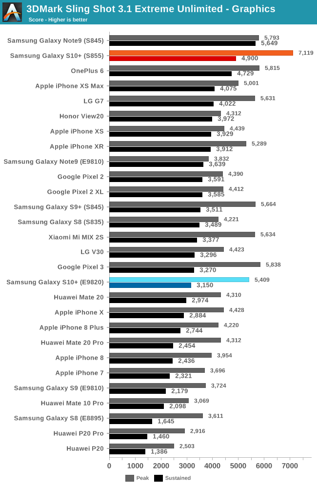
In the Graphics score of the workload, we come back to the familiar dominance of Qualcomm GPUs. What is interesting to see here is that both Galaxy S10 units sport worse sustained performance than the Note9 with last year’s chipsets. Most likely this is due to different thermal limits on these two Samsung devices.
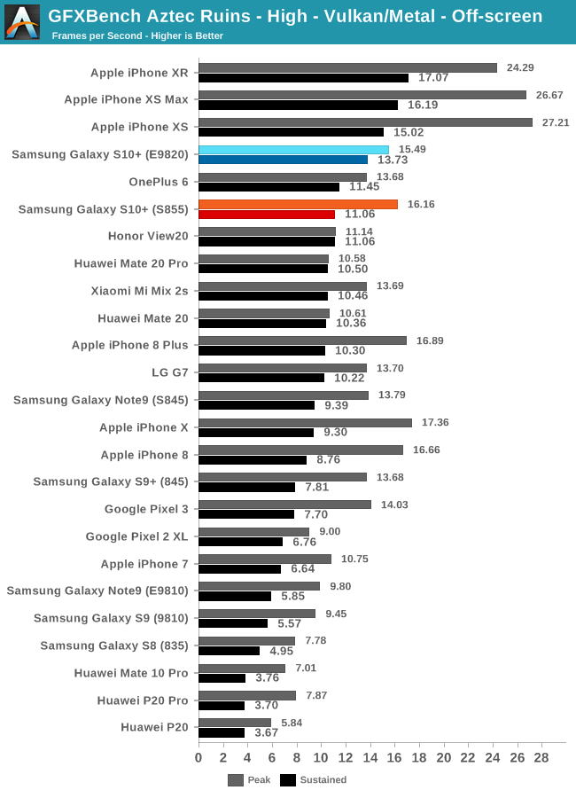
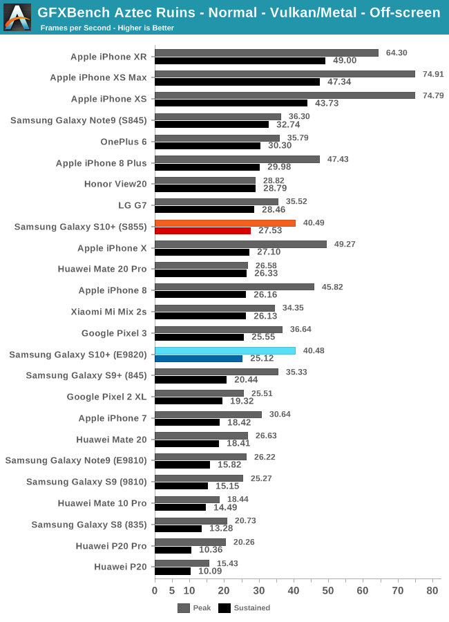
In the new GFXBench Aztec Ruins tests, the Exynos unit takes the lead in terms of sustained performance in the High variant test, only beaten by Apple’s newest iPhones. The phone doesn’t seem to reproduce the same lead in the Normal variant and subsequently slightly trails the Snapdragon 855 version. In sustained performance, the Exynos S10 beats last year’s predecessors, however the Qualcomm chip merely matches some of the better Snapdragon 845 devices from last year.
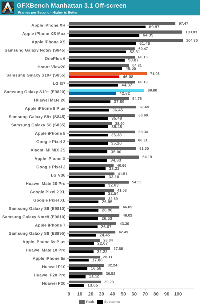
In Manhattan 3.1 Off-screen, we see both S10’s neck-in-neck in peak performance, and sustained performance also doesn’t seem all that different. The Exynos variant again shows big leaps over last year’s G72MP18 GPU, and the Qualcomm variant again is only able to match or actually lose out to some of the more thermally aggressive Snapdragon 845 units from last year.
| GFXBench Manhattan 3.1 Offscreen Power Efficiency (System Active Power) |
||||
| Mfc. Process | FPS | Avg. Power (W) |
Perf/W Efficiency |
|
| iPhone XS (A12) Warm | 7FF | 76.51 | 3.79 | 20.18 fps/W |
| iPhone XS (A12) Cold / Peak | 7FF | 103.83 | 5.98 | 17.36 fps/W |
| Galaxy 10+ (Snapdragon 855) | 7FF | 70.67 | 4.88 | 14.46 fps/W |
| Galaxy 10+ (Exynos 9820) | 8LPP | 68.87 | 5.10 | 13.48 fps/W |
| Galaxy S9+ (Snapdragon 845) | 10LPP | 61.16 | 5.01 | 11.99 fps/W |
| Huawei Mate 20 Pro (Kirin 980) | 7FF | 54.54 | 4.57 | 11.93 fps/W |
| Galaxy S9 (Exynos 9810) | 10LPP | 46.04 | 4.08 | 11.28 fps/W |
| Galaxy S8 (Snapdragon 835) | 10LPE | 38.90 | 3.79 | 10.26 fps/W |
| LeEco Le Pro3 (Snapdragon 821) | 14LPP | 33.04 | 4.18 | 7.90 fps/W |
| Galaxy S7 (Snapdragon 820) | 14LPP | 30.98 | 3.98 | 7.78 fps/W |
| Huawei Mate 10 (Kirin 970) | 10FF | 37.66 | 6.33 | 5.94 fps/W |
| Galaxy S8 (Exynos 8895) | 10LPE | 42.49 | 7.35 | 5.78 fps/W |
| Galaxy S7 (Exynos 8890) | 14LPP | 29.41 | 5.95 | 4.94 fps/W |
| Meizu PRO 5 (Exynos 7420) | 14LPE | 14.45 | 3.47 | 4.16 fps/W |
| Nexus 6P (Snapdragon 810 v2.1) | 20Soc | 21.94 | 5.44 | 4.03 fps/W |
| Huawei Mate 8 (Kirin 950) | 16FF+ | 10.37 | 2.75 | 3.77 fps/W |
| Huawei Mate 9 (Kirin 960) | 16FFC | 32.49 | 8.63 | 3.77 fps/W |
| Huawei P9 (Kirin 955) | 16FF+ | 10.59 | 2.98 | 3.55 fps/W |
Looking at the power consumption and efficiency tables in Manhattan 3.1, we see both devices showcase quite similar characteristics. Performance is very close in both chipsets, with also very similar power consumption within 220mW of each other. The efficiency also is quite close to each other. Interestingly both Qualcomm and Samsung weren’t able to close the gap to Apple’s latest iPhones and the A12 which still has a considerable performance and power efficiency lead.
For the Exynos chipset, it’s also unfortunate to see that absolute power has gone up by 1W, meaning the device will heat up faster, even though performance and efficiency is better.
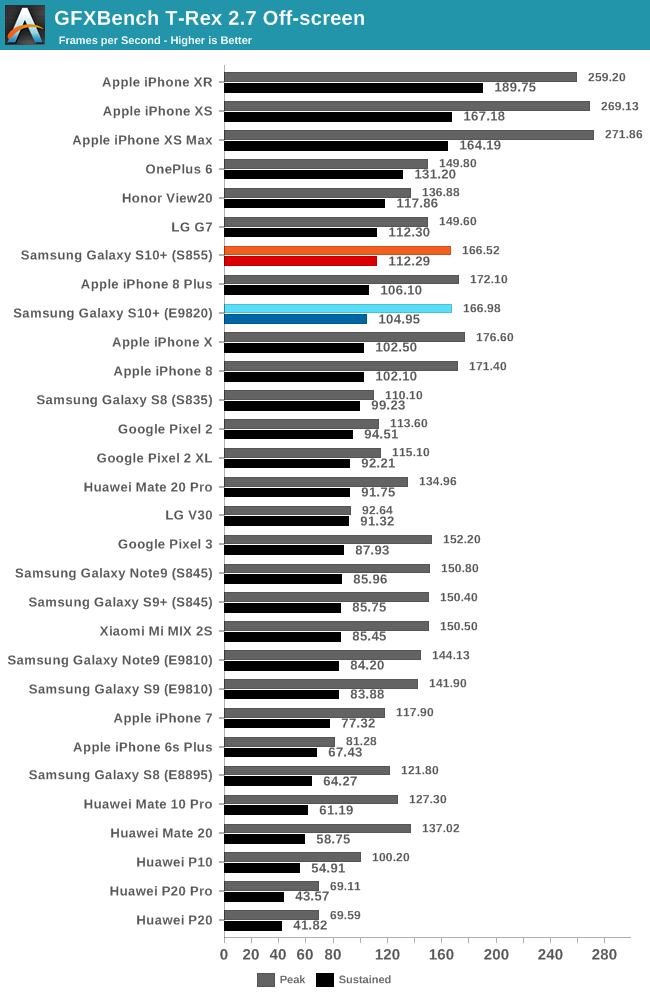
In T-Rex we again see both chipsets perform very similarly with similar sustained performance figures.
| GFXBench T-Rex Offscreen Power Efficiency (System Active Power) |
||||
| Mfc. Process | FPS | Avg. Power (W) |
Perf/W Efficiency |
|
| iPhone XS (A12) Warm | 7FF | 197.80 | 3.95 | 50.07 fps/W |
| iPhone XS (A12) Cold / Peak | 7FF | 271.86 | 6.10 | 44.56 fps/W |
| Galaxy 10+ (Snapdragon 855) | 7FF | 167.16 | 4.10 | 40.70 fps/W |
| Galaxy S9+ (Snapdragon 845) | 10LPP | 150.40 | 4.42 | 34.00 fps/W |
| Galaxy 10+ (Exynos 9820) | 8LPP | 166.00 | 4.96 | 33.40fps/W |
| Galaxy S9 (Exynos 9810) | 10LPP | 141.91 | 4.34 | 32.67 fps/W |
| Galaxy S8 (Snapdragon 835) | 10LPE | 108.20 | 3.45 | 31.31 fps/W |
| Huawei Mate 20 Pro (Kirin 980) | 7FF | 135.75 | 4.64 | 29.25 fps/W |
| LeEco Le Pro3 (Snapdragon 821) | 14LPP | 94.97 | 3.91 | 24.26 fps/W |
| Galaxy S7 (Snapdragon 820) | 14LPP | 90.59 | 4.18 | 21.67 fps/W |
| Galaxy S8 (Exynos 8895) | 10LPE | 121.00 | 5.86 | 20.65 fps/W |
| Galaxy S7 (Exynos 8890) | 14LPP | 87.00 | 4.70 | 18.51 fps/W |
| Huawei Mate 10 (Kirin 970) | 10FF | 127.25 | 7.93 | 16.04 fps/W |
| Meizu PRO 5 (Exynos 7420) | 14LPE | 55.67 | 3.83 | 14.54 fps/W |
| Nexus 6P (Snapdragon 810 v2.1) | 20Soc | 58.97 | 4.70 | 12.54 fps/W |
| Huawei Mate 8 (Kirin 950) | 16FF+ | 41.69 | 3.58 | 11.64 fps/W |
| Huawei P9 (Kirin 955) | 16FF+ | 40.42 | 3.68 | 10.98 fps/W |
| Huawei Mate 9 (Kirin 960) | 16FFC | 99.16 | 9.51 | 10.42 fps/W |
In the power end efficiency tables we however see a big difference between the two devices. Here Qualcomm is able to clearly achieve lower power and higher efficiency than the Exynos.
One thing that I note on both Galaxy S10 units is that I again saw some very odd thermal behaviour on the part of the Qualcomm unit. Just like we measured on the Note9 a few months ago, the Qualcomm Galaxy S10+ reached much higher initial temperatures than the Exynos S10+. I measured peak skin temperatures on the front screen near the SoC nearing 49°C on the S855 unit while the E9820 peaked around 43°C. Again, much like last year, this seems to be a time-bound boost mechanism as after a certain period of around 20 minutes the Snapdragon unit throttles down to a sustained 42-43°C. What this means is that the Snapdragon unit has higher (longer) peak performance figures at a cost of a hotter device, before both devices equalise at a sustained ~42°C.
Overall, the Snapdragon unit this year does still have a performance and efficiency lead, however the gap has been narrowed compared to what we’ve seen in the past years. The new Mali G76 looks to have made solid improvements, and ALU heavy heavy workloads in particular have seen very large leaps compared to the Exynos 9810. The Adreno 640 this generation just seems quite conservative – Apple has taken Qualcomm’s performance crown in mobile and most importantly also the efficiency crown. Both the Snapdragon 855 and A12 are both manufactured on the same process node so it’s a valid Dragon-to-Apples comparison, and here Qualcomm is beaten by such a significant margin of which in the past we’ve only been used to seeing Qualcomm beat Arm with. For the next generation, we thus hope both Qualcomm and Arm will be able to show more significant jumps in both performance and efficiency. Samsung’s own GPU is also a wildcard, however I’m not expecting to see this productised in next year’s Exynos.
On the new Galaxy S10, the display is the centre-piece of the phone. Samsung in particular has proclaimed some big new improvements in terms of brightness and display quality, advertising the HDR10+ capabilities of the screen.
One thing that Samsung didn’t mention is that this is the first Galaxy device shipping with Android’s new colour management support out of the box. What this means is that we have support for both standard gamut as well as wide-gamut content without switching between display modes in the settings. This latter menu has been redesigned in the Galaxy S10: gone are the familiar display modes such as Cinema, AMOLED Cinema or AMOLED Photo. The new S10 instead simply ships with a mere two modes: “Natural” and “Vivid”.
The natural mode is the default that the devices comes in, and is also the accurate CMS profile of the phone. This also means that Samsung now finally ships an accurate targeting display mode out of the box, targeting both sRGB and Display P3 gamuts (I didn’t test wider gamuts!).
The Vivid mode is a super-wide gamut near the native capability of the panel, the colours here don’t adhere to any specific display standard and are just meant for punchier colours which some users enjoy.
We move on to the display calibration and fundamental display measurements of the S10 screen. As always, we thank X-Rite and SpecraCal, as our measurements are performed with an X-Rite i1Pro 2 spectrophotometer, with the exception of black levels which are measured with an i1Display Pro colorimeter. Data is collected and examined using SpectraCal's CalMAN software.
The Galaxy S10’s brightness was something that was much touted during the launch of the phone. Here Samsung had advertised “peak brightness of up to 1200 nits”. This figure was sourced by DisplayMate’s testing, however it’s a pretty misleading number as the phone only achieves this at minimal APL, which is nearly impossible to achieve in real life usage.
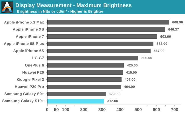
In regular scenarios, the Galaxy S10’s maximum brightness is similar to that we’re used to from past Samsung phones, reaching a maximum of 310-320nits.
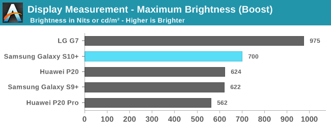
To achieve brightness higher than this, the phone needs to be in adaptive brightness mode and in high ambient light. Here the Galaxy S10+ reaches up to around 700nits. I’ve tested this on both my units and got matching maximum brightness figures.
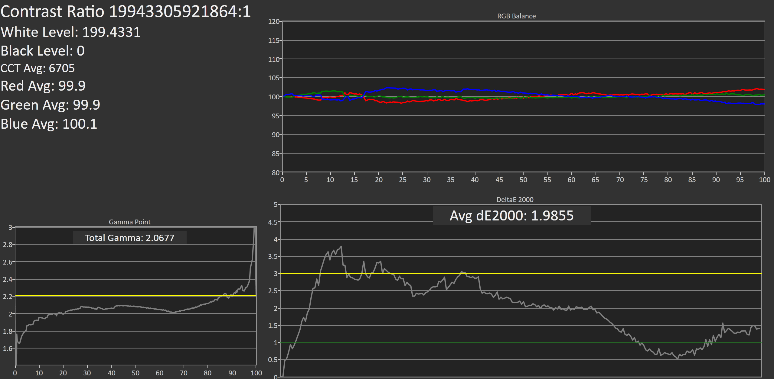
SpectraCal CalMAN
Exynos Natural
Exynos Vivid
Snapdragon Natural Snapdragon Vivid
Greyscale accuracy measurements on the Galaxy S10+ ended up being quite a headache because the Exynos and Snapdragon units behaved very differently. The issue at hand wasn’t any manufacturing divergence on the part of the panel, but rather an issue of diverging software calibrations between the different models and display modes. To make things even more annoying, the Galaxy S10 is also Samsung’s first smartphone with very aggressive CABC (Content adaptive brightness control) which cannot be turned off, with brightness scaling very differently based on APL.
At 200 cd/m² on both Exynos and Snapdragon units in Natural mode we see too warm white colour balance, with especially dominating reds, resulting in colour temperatures of 6327K and 6250K for each respective unit. In Vivid mode, oddly enough the Snapdragon was warmer at 6945K while the Exynos had a more blue 7697K CCT. It’s to be noted that in Vivid mode Samsung allows users to adjust the colour temperature, whilst this isn't possible in Natural mode.
What is inherently broken on both phones in different modes are the gamma curves. On the Exynos unit the natural mode has a far too low gamma at low levels and too high on high levels. In Vivid mode this low gamma on the low-end is reversed, with some additional black clipping now due to too high gamma, with again too high gamma at the high levels.
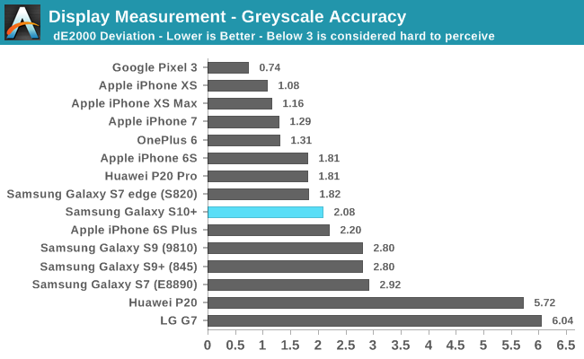
On the Snapdragon unit, the natural mode is the only display mode out of all combinations that actually manages to have a correct gamma near 2.2, with the only issue being a slight amount of black clipping at the lower levels. This is the mode and device with the best greyscale dE2000 of 1.79 – only thwarted from getting a better score due to the overly red colour temperature.

Exynos Gamma Problem
The gamma issues on the Exynos variant in natural mode are especially apparent in the most ironic place: Samsung’s own display mode settings screen. When enabling Night Mode in OneUI and using the dark interface, the background isn’t actually black but of a very low level grey. It’s exactly at these levels where the gamma differences between the Natural and Vivid display become obviously apparent. The above GIF shows how the broken low gamma in natural mode makes the UI exceedingly brighter. On the Snapdragon unit of the Galaxy S10, and for that matter the S9 and Note9 as well, we don’t encounter this change in gamma when switching between display modes and the Night Mode UI remains of an extremely dark grey nearing true black.
We end up with four different greyscale comparison patterns:
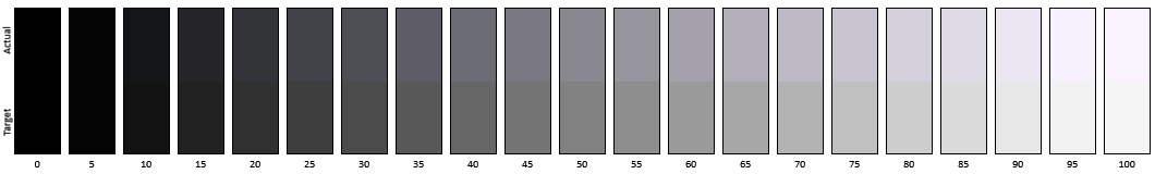
SpectraCal CalMAN - Exynos Vivid
The Exynos in Vivid mode is too blue with too dark mid to high level tones.
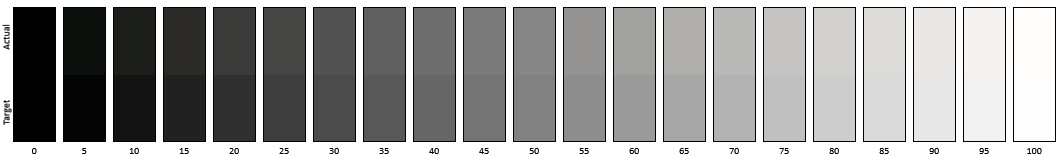
SpectraCal CalMAN - Exynos Natural
The Exynos in natural mode is unperceivably red, however we can clearly see too bright tones above what they normally should be.

SpectraCal CalMAN - Snapdragon Vivid
The Snapdragon in Vivid mode is ever so slightly too blue, but the gamma is off and again too dark.
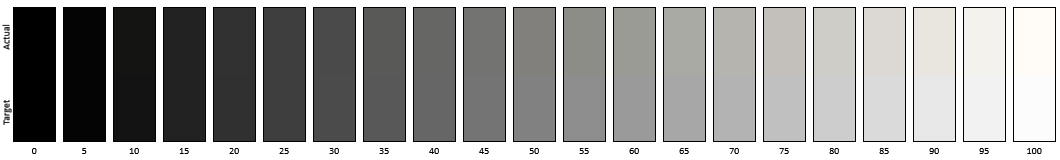
SpectraCal CalMAN - Snapdragon Natural
Finally, the Snapdragon in Natural mode is the only mode that is near perfect, with correct gamma and an hard to perceive slight shift towards red.

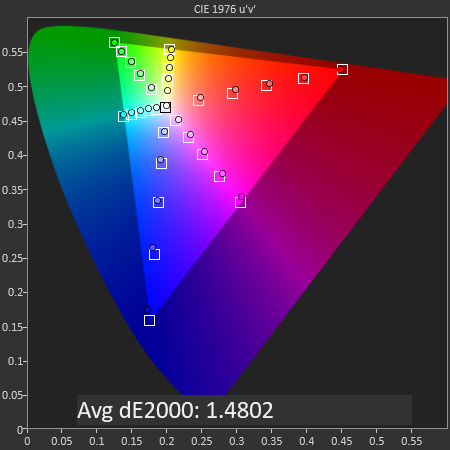
SpectraCal CalMAN
Exynos - Snapdragon
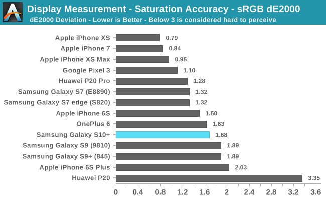
Continuing with saturation accuracy measurements, we see that in that in Natural mode on both phones we’re getting similar results with dE2000 deviations of 1.68 for the Exynos and 1.48 for the Snapdragon. Both phones share the same issue of having offset red mid-level saturations.

SpectraCal CalMAN
Exynos - Samsung S-Browser
Testing the Display P3 patterns in Natural mode is a bit of a headache. Samsung introduced colour management with the Galaxy S10, however there’s one gigantic caveat: The OS can’t display content of different gamuts alongside each other. For example, viewing P3 pictures in Samsung’s default S-Browse results in incorrectly clipped saturations, and in effect the browser is still limited to sRGB content.
Out of all applications I’ve tested on the Galaxy S10, Samsung’s only app that supports wide gamut content is the Gallery app, but again with a big caveat. It only switches over to wide gamut when opening up a picture, and when in thumbnail mode the content is still limited to sRGB. Apple’s iPhone Photos app doesn’t have this issue and is able to display P3 thumbnails alongside sRGB thumbnails.
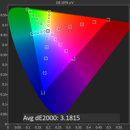

SpectraCal CalMAN
Exynos - Samsung Gallery vs Chrome P3 Forced
To make matters worse, the actual rendering of P3 content though the OS is actually incorrect. Displaying P3 patterns in the Gallery app results in a dE of 3.18, which at the limit of what should be acceptable. However if we completely bypass Android’s internal CMS transform and instead of rely on an external app, we can achieve some great results. In this case we rely on Chrome and tell it to force itself to D65 P3 display mode, and through this we’re measuring the Galaxy S10’s panel with a fantastic dE2000 of 1.03, as good as Apple’s best performance in the iPhone XS.
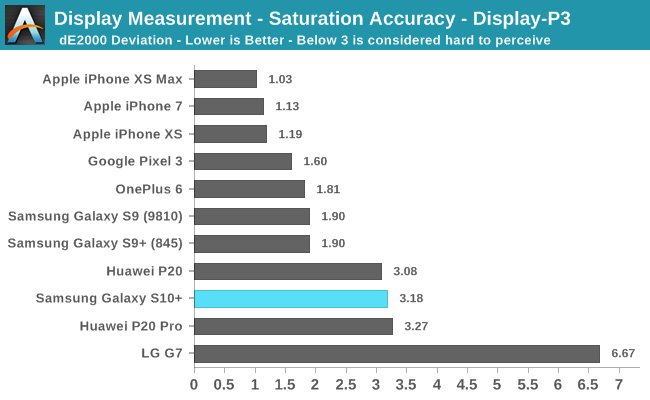
In the end, because most users will be using P3 content through the default CMS, the Galaxy S10+ ends up with a disappointing dE of 3.18.
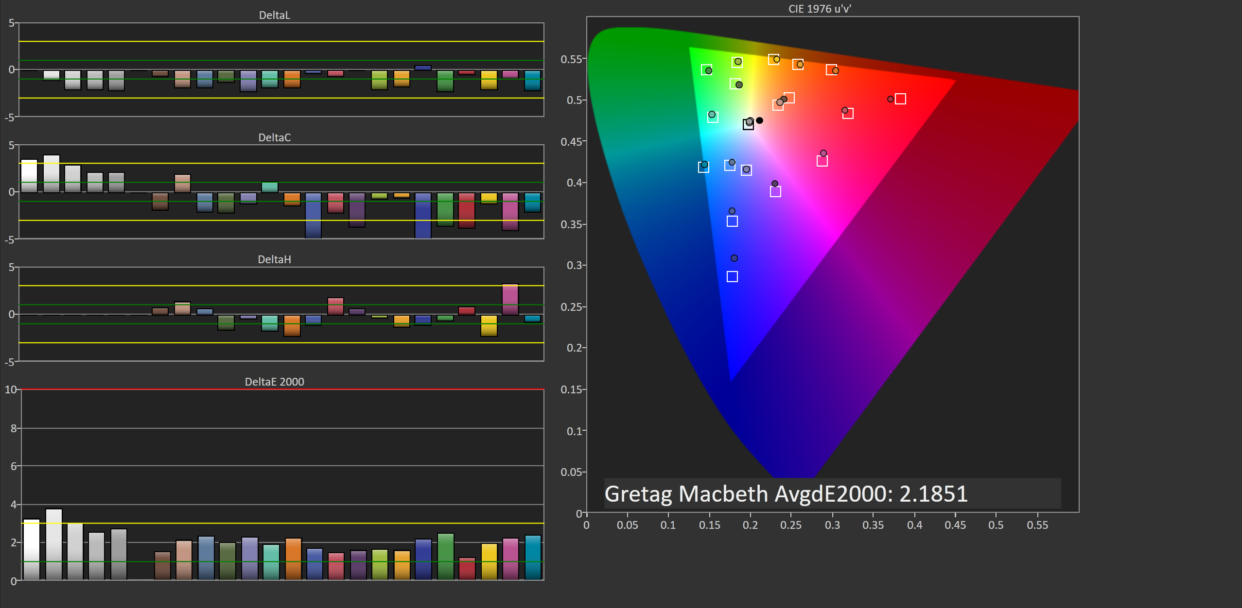
SpectraCal CalMAN
SpectraCal CalMAN
Exynos
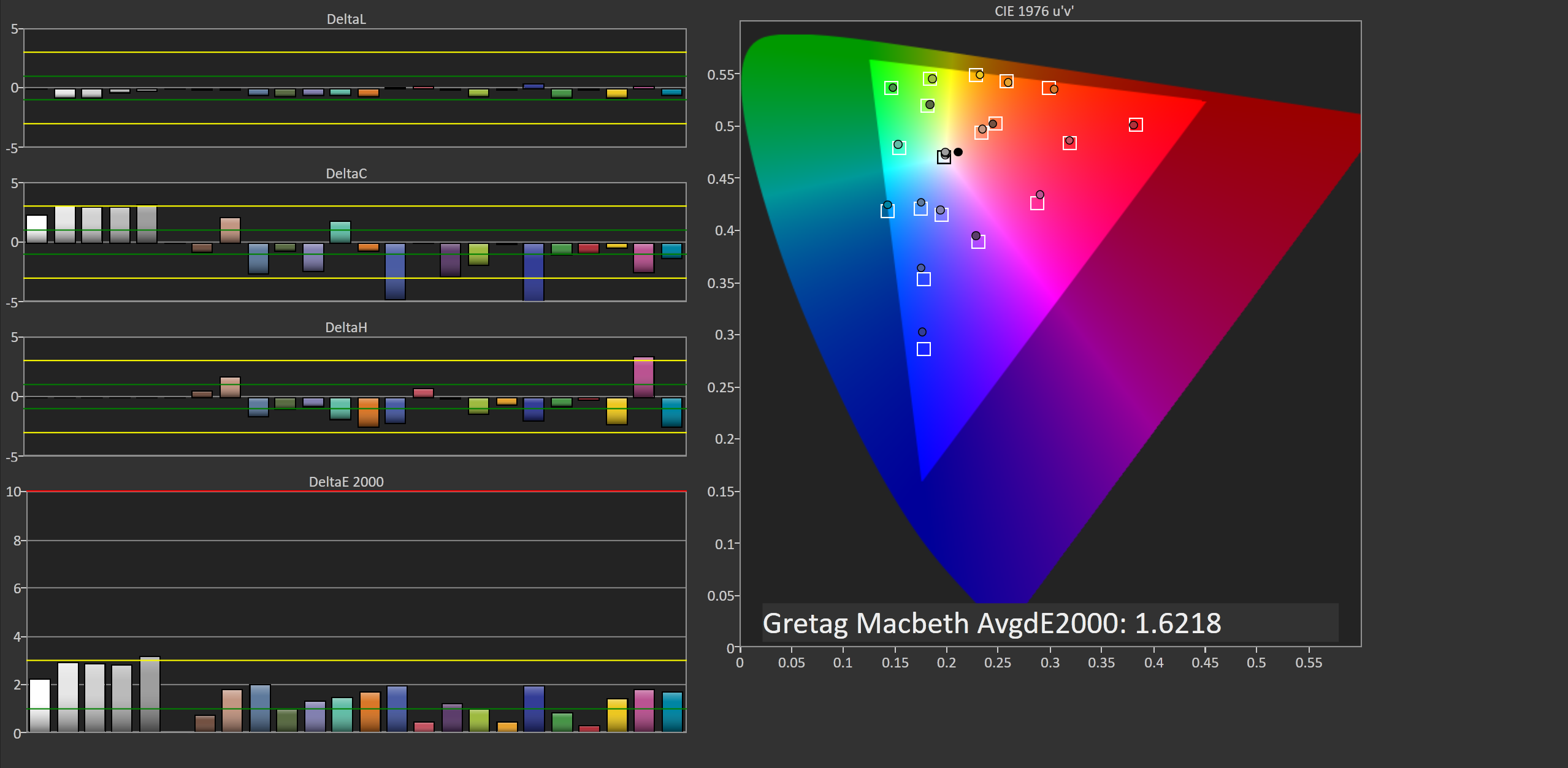
SpectraCal CalMAN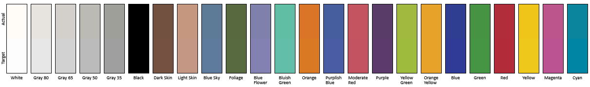
SpectraCal CalMAN
Snapdragon
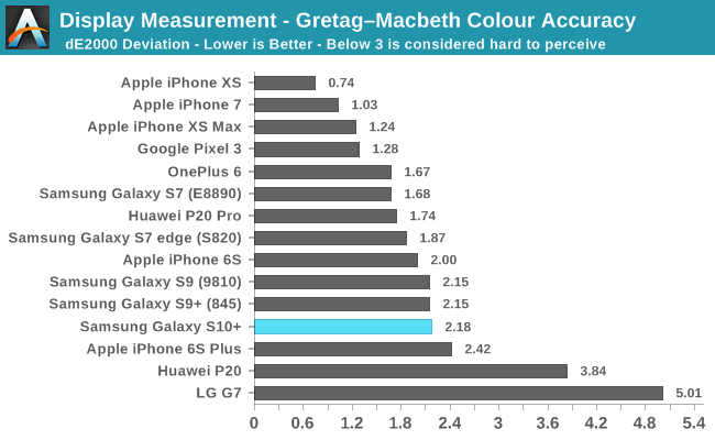
Finally, in the Gretag-Macbeth test of common found tones we see a case of the Exynos S10 scoring worse with a dE of 2.18 versus the Snapdragon’s figure of 1.62. In terms of hue, both display panels exhibit extremely similar characteristics in the test tones, but it’s again the flawed gamma on the Exynos unit which really offsets things and shows too bright results, compared to the Snapdragon’s near perfect gamma.
Display Conclusions
Overall, the Galaxy S10+’s display is a typical Galaxy S display. Samsung over the last 3 iterations has continued to have issues with their gamma, often times patching the most obvious issues a few months after release. While differences between the Exynos and Snapdragon calibrations have always been there, we’ve never had such a jarring issue as on the Exynos’ Natural mode. The other display modes including on the Snapdragon also continue to have black clipping at the first few greyscale levels. To be honest, this is getting a bit tiring and frankly I’m losing hope in Samsung to ever getting this right at release, it’s obvious that the quality control in their calibration department just isn’t there and after so many years of the same issues the company obviously doesn’t care to improve things.
Samsung adopting Android’s CMS in the Galaxy S10 also is of mixed feelings. Actually the S10 shipped with the traditional various mDNIe scenarios we’re used to from Samsung, but they’re just unavailable from the settings UI. Thus I think the decision to have the phone released with the CMS must have been a last minute choice. The biggest caveat here is the fact that Android cannot display different gamuts alongside each other, and fundamentally this is an issue of Android, Google and maybe even the SoC vendors. For now, Apple is 4 years ahead of everybody else and there’s yet to be an Android phone matching the iPhone’s colour management capabilities.
Having said all of the negative things, the Galaxy S10 with all its issues still probably remains among the best displays available. It’s a step down from the S9 and Note9 in terms of calibration, but all other aspects such as display sharpness, viewing angles, brightness and naturally contrast are just top-notch for the new Galaxy S10.
Battery performance of the Galaxy S10+ has been touted to be as class-leading. The introduction of a larger battery, more efficient screen as well as a new generation of SoCs are sure to bring improvements over last year’s Galaxy S9. One aspect that readers will have waited for impatiently is our testing of the new Exynos 9820 variant against the Snapdragon 855, which has also been one topic I’ve been extremely interested to see.
Without further ado, let’s get do the results:
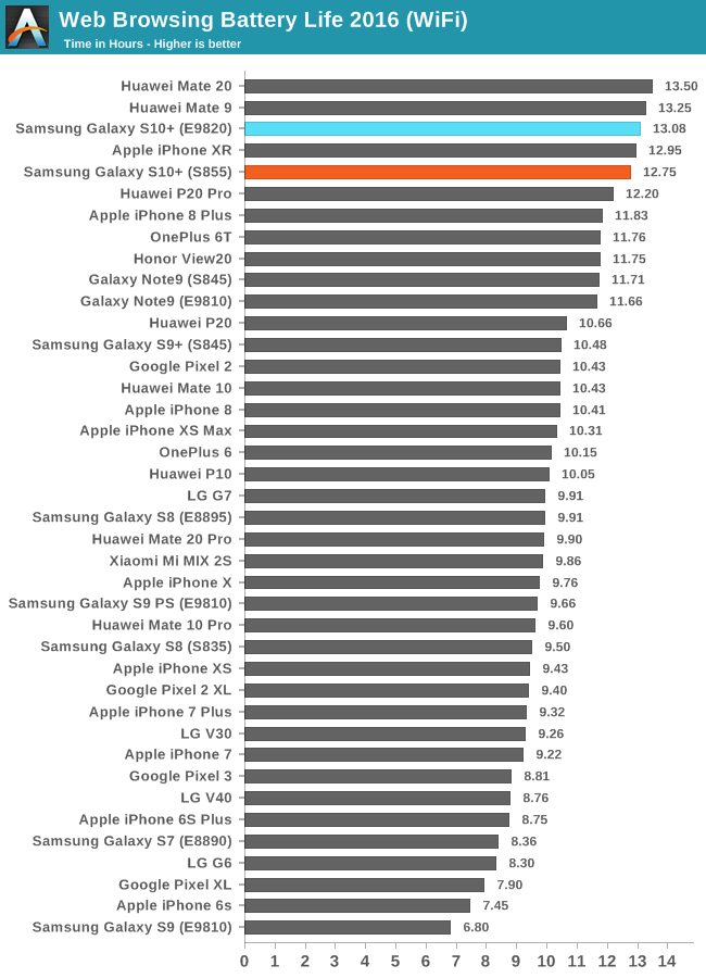
In our web browsing test, both Galaxy S10+s are showcasing outstanding longevity at 13.08h for the Exynos and 12.75h for the Snapdragon variant. Least to say, I was extremely surprised to see this result even though we measured the Exynos 9820 CPU to be quite less efficient than the Snapdragon 855 in peak performance efficiency. I would have not expected the Exynos to match the Snapdragon, much less slightly beat it.
Before going into more details, let’s see the PCMark battery test results:
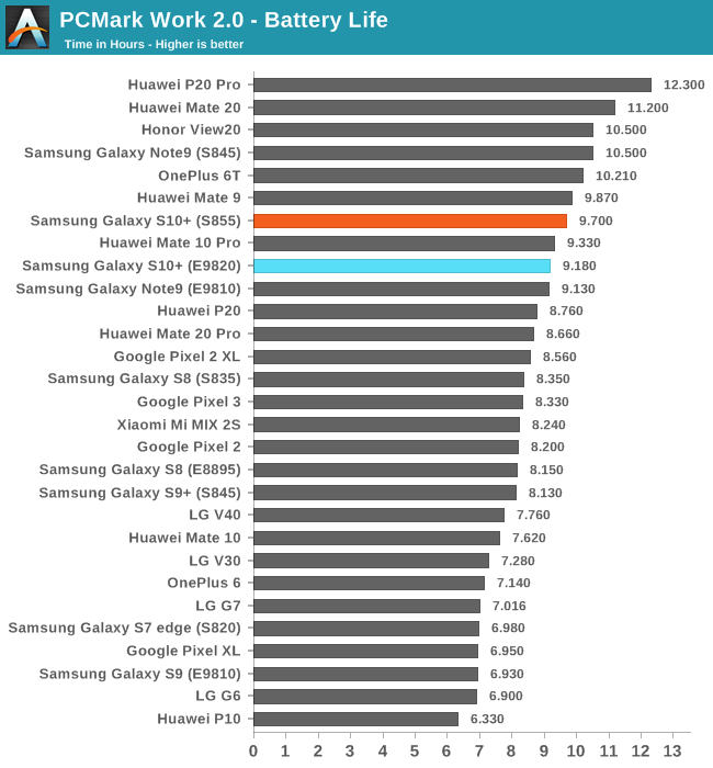
Here, in absolute terms, the Galaxy S10+ aren’t quite as impressive as on the web test and further lag behind the excellent results of the Kirin 980 devices. Nevertheless, these are some impressive figures and again it’s very good to see that both units are almost evenly matched, this time the Snapdragon unit lasting slightly longer than the Exynos.
To explain these results, we have to keep one thing in mind: the Exynos unit will have posted worse performance than the Snapdragon, so it will have spent more time at the lower more efficient frequency states.
One thing that I also noticed, is that in very low idle loads where there’s just some light activity on the A55 cores, the Exynos 9820 variant actually uses less power than the Snapdragon unit. The figures we’re talking about here are 20-30mW, but could possibly grow to bigger values at slightly more moderate loads. It’s possible that Qualcomm has more static leakage to deal with on the 7nm process than Samsung on 8nm, one thing that I’ve come to hear about the TSMC 7nm node.
Furthermore, one of the biggest improvements for the Galaxy S10 over past devices isn’t actually the SoC nor the actual bigger battery. It’s actually the display as well as the base power consumption of the phone. In Airplane mode, the base power has gone down by almost 100mW compared to the Galaxy S9+ which is a fantastic development and is especially something that will result in higher low-brightness battery life.
Currently in my time with both S10+ units, I can say they’ve been among the longest lasting Android devices I’ve tested.

Exynos vs Snapdragon in identical usage patterns & Prolonged idle periods
One issue I can confirm with the Exynos unit is that after a voice call in any app, the phone isn’t correctly entering its lower power state, and will suffer from increased idle battery drain until a reboot. This is something that hopefully Samsung addresses in a firmware update as it doesn’t look to be a hardware related issue. When not affected by this bug, both phones idle very similar to each other and slightly better than the S9+ I use as my daily device.
Besides the display of the Galaxy S10, the biggest new features of this year’s flagship is the camera setup. The S10 is Samsung’s first flagship device with a triple-camera setup, and also the first Samsung flagship a wide-angle camera module.
The main camera module in terms of specifications is similar to last year’s: A 12.2MP sensor taking still pictures up to a resolution of 4032 x 3024. The focal length is 26mm, or a FoV of 77° and the lens mechanism comes with Samsung’s signature dual-aperture mode with f/1.5 and f/2.4 apertures. The sensor has 1.4µm pixels with full dual-pixel PDAF. Even though Samsung doesn’t advertise it, the sensor actually did see a change this year. S.LSI actually seemingly has won the design contract for all main sensors on the S10, coming with a new “S5K2L4” sensor shared among both Snapdragon and S.LSI variants.
The telephoto lens also remains a similar 12MP unit with 1.0µ pixels with a 52mm focal length or 45° FoV which acts as a 2x telephoto lens and an aperture of f/2.2. I wasn’t able find the sensor name for this module.
Finally the new wide-angle module is a 16MP shooter with 1.0µm pixels and a 13mm / 123° wide angle view on an f/2.4 aperture lens. The notable part about this unit is that it lacks any autofocus mechanism and also doesn’t come with OIS like the other two rear camera modules. The sensor here is again supplied by SLSI and is the “S5K3P9”.
Sony apparently just won dual-sourcing of the main front 10MP sensor in the form of the IMX374 which is shared with S.LSI’s S5K3J1. Oddly enough the secondary front camera / depth sensor is reported as 6.5MP which doesn’t match Samsung’s official specifications of it being 8MP.
This year I had a hunch about the camera performance between the Snapdragon and Exynos units and actually made the effort to wait for my camera evaluation until I got both units in-house (Plus the weather was bad for a week!). In the past there were some slight discrepancies between the two chipset variants but never something to really worry about. As we’ll see for the Galaxy S10 – this is absolutely not the case and the Snapdragon 855 Galaxy S10+ versus the Exynos Galaxy S10+ will be showcasing some drastic differences in camera performance.

[ Galaxy S10+ Snapdragon ] - [ Galaxy S10+ Exynos ]
[ Galaxy Note9 (E) ] - [ Galaxy S9+ (S) ] - [ Galaxy S8 ]
[ iPhone XS ] - [ iPhone X ] - [ LG V40 ] - [ OnePlus 6T ]
[ Pixel 3 ] - [ View20 ] - [ Mate 20Pro ]
In the main module we’re seeing some slight exposure differences between the two units; the Snapdragon is able to maintain more contrast in the picture as the Exynos’ HDR flatten things a bit too far. The Snapdragon’s exposure is nearly identical to the S9+ and at first glance it’s hard to see any difference.
Opening up the full resolution images however shows a definitive change in details, with the Galaxy S10 actually see a degradation compared to the S9+. This is particularly visible in the trees on the right part of the scene where the S10 blurs the branches a lot more. The same degradation also happens against the Note9 which in these shots is the Exynos variant, so I don’t think it’s something related to the new S.LSI sensor vs the S9+’s Sony sensor.
Switching over the zoom and wide angle lenses, the difference between the Snapdragon and Exynos S10 is massive. What especially is striking is the colour rendition between both phones. The Snapdragon is a lot more saturated with stronger contrasts in textures. In the zoom shot the Exynos, while maybe being more natural, looks just bland and lacking saturation compared to the Snapdragon’s more colourful rendition with a ton more texture contrast. In the wide-angle shot, the Exynos also vastly loses out in detail in the trees in the right part of the scene, ending up as a smudged result while the Snapdragon maintain the branch detail.
Comparing the wide-angle shots against the competition, only real competitor is the Mate 20 Pro as the LG V40 continues to apply LG’s pointless blurring noise reduction which results in a water-colour effect.

[ Galaxy S10+ Snapdragon ] - [ Galaxy S10+ Exynos ]
[ Galaxy Note9 (E) ] - [ Galaxy S9+ (S) ] - [ Galaxy S8 ]
[ iPhone XS ] - [ iPhone X ] - [ LG V40 ] - [ OnePlus 6T ]
[ Pixel 3 ] - [ View20 ] - [ Mate 20Pro ]
In the next shot we again see big differences in the HDR between the two phones. The Snapdragon unit has a lot more colour and contrast. There’s some odd effect going on with the detail of the gravel in the Snapdragon as the Exynos looks more natural, however in other parts of the scene detail definitely goes to the Snapdragon unit. The Exynos S10 is definitely a downgrade compared to the S9+.
The main competitions to the S10’s are the iPhone XS and V40’s main cameras. Comparing the XS picture, it’s obvious to see that the S10 applies a very large amount of sharpening which also results in a lot of halo artefacts around contrasted edges. This is one aspect in which the Exynos S10 seems to do better as its sharpening looks less aggressive, and thus for example the gravel looks better in this variant of the S10.
In the wide-angle shot we see similar results: The Qualcomm unit has massively better shadows and maintaining detail in the foliage in the scene. The Mate 20 Pro would have been a contender, however it missed the mark in terms of colour temperature, and the LG V40’s detail processing shoots itself in the foot as it for example just washes away the gravel.
[ Galaxy S10+ Snapdragon ] - [ Galaxy S10+ Exynos ]
[ Galaxy Note9 (E) ] - [ Galaxy S9+ (S) ] - [ Galaxy S8 ]
[ iPhone XS ] - [ iPhone X ] - [ LG V40 ] - [ OnePlus 6T ] - [ Pixel 3 ]
[ View20 ] - [ Mate 20Pro ]
Under the bridge HDR is again extensively used. The Qualcomm variant is able to achieve yet again more texture contrast and thus the bricks are more defined. To be noted is that both units had the same exposure time and ISO. The Snapdragon is a bit too colourful here with the sandstone while the Exynos is too bland.
In the wide angle, one would have thought the phones reversed as it’s the Exynos providing a more contrastful image and bringing out the textures. The Snapdragon is a lot more sharp as maintains the tree branches much better.
The Mate 20 Pro’s wide angle shot is a bit darker however it handily beats out the S10+ in terms of textures and detail. The V40 yet again almost completely blurs out the bricks in this shots in some spots so let’s just ignore it going forward.

[ Galaxy S10+ Snapdragon ] - [ Galaxy S10+ Exynos ]
[ Galaxy Note9 (E) ] - [ Galaxy S9+ (S) ] - [ Galaxy S8 ]
[ iPhone XS ] - [ iPhone X ] - [ LG V40 ] - [ OnePlus 6T ]
[ Pixel 3 ] - [ View20 ] - [ Mate 20Pro ]
In the city shot, the Exynos slightly flattens highlights too much and the building’s sunlit façade is toned down too much, the Snapdragon is doing better in maintaining the natural brightness. The Snapdragon did have a longer exposure however the main differences area in the processing.
On the wide-angle, the Exynos has more contrast, however it’s the bad kind of contrast due to lower dynamic range. The shadows in the scene lack definition as seen in the balconies, and again there’s such a big difference in detail retention between the two that I’m starting to wonder if there’s anything wrong with the optics on the Exynos, however we see this happening even in the centre of the image as well.
The Mate 20 Pro’s wide angle here is still clearly better than the S10 as it provides my dynamic range as well as a lot sharper details and textures.

[ Galaxy S10+ Snapdragon ] - [ Galaxy S10+ Exynos ]
[ Galaxy Note9 (E) ] - [ Galaxy S9+ (S) ] - [ Galaxy S8 ]
[ iPhone XS ] - [ iPhone X ] - [ LG V40 ]
[ OnePlus 6T ] - [ Pixel 3 ]
[ View20 ] - [ Mate 20Pro ]
This is a good shot to compare main, zoom and wide angle lenses and really showcases the advantages of having three camera modules.
As the scene has less HDR processing in general, the differences in exposure between the two S10s are less pronounced as in the previous shots. But even here the Snapdragon has some advantages such as the detail retention on the left tree.
In the wide angle shot the Exynos has significantly more noise in the blue sky even though both sensors captured at the same ISO and exposure length.

[ Galaxy S10+ Snapdragon ] - [ Galaxy S10+ Exynos ]
[ Galaxy Note9 (E) ] - [ Galaxy S9+ (S) ] - [ Galaxy S8 ]
[ iPhone XS ] - [ iPhone X ] - [ LG V40 ]
[ OnePlus 6T ] - [ Pixel 3 ]
[ View20 ] - [ Mate 20Pro ]
I the last scenic shot the composition between both S10’s is very similar however we see much better shadow detail in the low left on the Snapdragon unit. Throughout the picture the Snapdragon is also sharper although it does look like it might be a post-processing effect, even if it is I find it overall positive for the result.
The S9+ with the Sony sensor I think still provides the best natural sharpness and would choose that aspect over the S10’s result, even though the S10 has better dynamic range exposure.
On the wide angle, we see the Snapdragon have lighter shadows however the Exynos brings out more textures on the same spots. This shot also makes me think again there’s something wrong with the optics on the Exynos variants as details off-centre are just blurry and typical of lens issues we’ve seen in problematic smartphones over the years.
In terms of detail in the shop window here the Snapdragon has very slight advantages. It also has more saturated colours, however it doesn’t exaggerate them.

[ Galaxy S10+ Snapdragon ] - [ Galaxy S10+ Exynos ]
[ Galaxy Note9 (E) ] - [ Galaxy S9+ (S) ] - [ Galaxy S8 ]
[ iPhone XS ] - [ iPhone X ] - [ LG V40 ] - [ OnePlus 6T ]
[ Pixel 3 ] - [ View20 ] - [ Mate 20Pro ]
 [ Galaxy S10+ Snapdragon ] - [ Galaxy S10+ Exynos ]
[ Galaxy Note9 (E) ] - [ Galaxy S9+ (S) ] - [ Galaxy S8 ]
[ iPhone XS ] - [ iPhone X ] - [ LG V40 ] - [ OnePlus 6T ]
[ Pixel 3 ] - [ View20 ] - [ Mate 20Pro ]
The flower shot is more of a test of the sensor’s light capture ability as flowers reflect light in a very wide spectrum. There’s some slight differences in the S10 but nothing to really come to any conclusion.
Daylight Camera Conclusion
Overall, the camera evaluation of the Galaxy S10 was extremely revealing this generation. I would have not expected such big differences between the Exynos and Snapdragon units and this really exposes an issue which I think hadn’t been brought up before in such detail.
Clearly the HDR processing on the Snapdragon chip is superior, but the Snapdragon unit is also to resolve better details and also produces more (correctly) colourful images, whereas the Exynos can appear washed out an dull.
That being said, both units showcase huge improvements in their dynamic range capture ability which makes big jumps compared to past devices. One aspect of the Galaxy S10s that I saw was essentially flawless was the colour balance. In all the scenes I’ve shot in this evaluation I didn’t see one shot of the S10s where it was off in terms of colour reproduction (besides the Exynos’ sometimes dull saturations). In terms of shooting consistency as well, although both S10s differed between each other, in terms of consecutive shots this was probably Samsung’s best camera experience yet.
Exposure in particular is absolutely spot on. Many of the scenes were shot in on a day with no clouds at all with a very bright sun and here the S10 actually took advantage of the higher levels in the produces shots which some other phones don’t do. The Pixel 3 for example is a prime case of this as the last 10% of levels are almost never used which results in missing highlights in almost all shots, resulting in a dark image that just doesn’t make sense given the environment of the scene.
I really love these aspects about the Galaxy S10 camera in daylight shots as it produces just better shots.
The wide angle module is a fantastic addition to the phone. Previously only LG was able to sport such a feature, and the Mate 20’s from Huawei were the first to follow LG in this regard. I had mentioned that the Mate 20 Pro’s wide angle was excellent, however the only comparison point was LG’s own, which unfortunately suffers from processing issues. The S10’s wide angle beats both in many scenarios. It’s also on the wide angle where we see the most drastic differences between the two tested S10 models. One thing that I think is a hardware issue on the Exynos unit I’ve tested is the camera lens of the wide angle module as it’s showing very blurred details in off-centre details. Because the camera module is fixed focus, I don’t think this is something that will be fixed in any update.
Low-light capture improvements is something that Samsung has been very mum about for the Galaxy S10. Fundamentally on the hardware side of things nothing has really improved compared to the Galaxy S9/Note9. So in practise, any difference we would be seeing should be solely based on the processing improvements of the Galaxy S10.
[ Galaxy S10+ Snapdragon ] - [ Galaxy S10+ Exynos ]
[ Galaxy Note9 (E) ] - [ Galaxy S9+ (S) ] - [ Galaxy S8 ]
[ iPhone XS ] - [ iPhone X ] [ LG V40 ] - [ OnePlus 6T ]
[ Pixel 3 ] - [ View20 ] - [ Mate 20Pro ]
In the first shot, we’re seeing again very different results between the Snapdragon and Exynos, but in a twist compared to the daylight shots, this time around it’s an advantage on the side of the Exynos model. Here the latter models is able to bring out a lot more shadows in the scene and is significantly sharper than the Snapdragon variant. The Snapdragon does a bit better on the bright highlights of the signage, however I don’t think this was worth it as it gives up too much in other parts of the shot.
I feel as if the Snapdragon has quite a bit of sharpening going on, which makes very little sense to use in a scenario like this.
The Galaxy S10’s are both beat by the Mate 20 Pro’s large sensor which just has much better native dynamic range, retaining more texture details on the gas station floor and roof.
Using the wide-angle lens in such a scenario doesn’t result in very good picture. The Snapdragon achieves better dynamic range and able to show the signage correctly without overblowing it, however the Exynos beats it in terms of detail. Noise on the latter is a lore more coarse and pronounced which can result in some ugly regions on even surfaces.

[ Galaxy S10+ Snapdragon ] - [ Galaxy S10+ Exynos ]
[ Galaxy Note9 (E) ] - [ Galaxy S9+ (S) ] - [ Galaxy S8 ]
[ iPhone XS ] - [ iPhone X ] - [ LG V40 ] - [ OnePlus 6T ]
[ Pixel 3 ] - [ View20 ] - [ Mate 20Pro ]
Big advantages in sharpness on the bright parts of the picture for the Snapdragon with stronger contrast for this phone. The Exynos doesn’t do well on the bright parts, blurring them, but on the other hand it has better details in the shadows than the Snapdrgon, with overall less pronounced light noise.
In terms of light capture, the Mate 20 Pro is far ahead and Night Sight on the Pixel 3 also sweeps the floor with the competition.
[ Galaxy S10+ Snapdragon ] - [ Galaxy S10+ Exynos ]
[ Galaxy Note9 (E) ] - [ Galaxy S9+ (S) ] - [ Galaxy S8 ]
[ iPhone XS ] - [ iPhone X ] - [ LG V40 ] - [ OnePlus 6T ]
[ Pixel 3 ] - [ View20 ] - [ Mate 20Pro ]
The Snapdragon here is heavier processed with darker shadows and noise reduction, however this makes little sense in a low-light show and the Exynos is more natural with better shadow detail even if it has more natural sensor noise.
Although Samsung at least beats the newest iPhones, it’s no match for Huawei and the Pixel’s Night sight.

[ Galaxy S10+ Snapdragon ] - [ Galaxy S10+ Exynos ]
[ Galaxy Note9 (E) ] - [ Galaxy S9+ (S) ] - [ Galaxy S8 ]
[ iPhone XS ] - [ iPhone X ] - [ LG V40 ] - [ OnePlus 6T ]
[ Pixel 3 ] - [ View20 ] - [ Mate 20Pro ]

[ Galaxy S10+ Snapdragon ] - [ Galaxy S10+ Exynos ]
[ Galaxy Note9 (E) ] - [ Galaxy S9+ (S) ] - [ Galaxy S8 ]
[ iPhone XS ] - [ iPhone X ] - [ LG V40 ] - [ OnePlus 6T ]
[ Pixel 3 ] - [ View20 ] - [ Mate 20Pro ]
In the last generic low light shot we see the Snapdragon again favour evening out highlights and sacrificing shadows. The Exynos does the opposite with more blown out highlights but with better shadow detail retention in the foreground.
On the wide angle, the Exynos produces a much more useable shot even though the noise is quite terrible.

[ Galaxy S10+ Snapdragon ] - [ Galaxy S10+ Exynos ]
[ Galaxy Note9 (E) ] - [ Galaxy S9+ (S) ] - [ Galaxy S8 ]
[ iPhone XS ] - [ iPhone X ] - [ LG V40 ]
[ OnePlus 6T ] - [ Pixel 3 ]
[ View20 ] - [ Mate 20Pro ]
Going into extreme low light scenarios, we’re venturing into shots that usually in the past we didn’t expect phones to be able to capture.
This is the first scene in which Samsung’s new Bright Night mode triggers. The new extreme ultra low light mode functions similarly to Huawei’s Night mode or Google’s Night sight, although the results here aren’t quite the same. The result here heavily favour the Snapdragon chip as it’s able to produce much less noise. It’s not competing with Huawei or Google, however it is able to showcase a result that is much better than some other traditional shooters.

[ Galaxy S10+ Snapdragon ] - [ Galaxy S10+ Exynos ]
[ Galaxy Note9 (E) ] - [ Galaxy S9+ (S) ] - [ Galaxy S8 ]
[ iPhone XS ] - [ iPhone X ] - [ LG V40 ] - [ OnePlus 6T ]
[ Pixel 3 ] - [ View20 ] - [ Mate 20Pro ]
A second example of the new Bright Night mode, we again see that it does help the S10 over its auto mode and it lands the phone in third place after Huawei’s flagship and Google’s Night Sight.
Low-light Conclusion
Overall, the low-light capture ability of the Galaxy S10 isn’t very exciting. Fundamentally Samsung needed to innovate more in this regard and I would have wanted to see some more innovation to the likes of Huawei and Google.
Low-light is again a scenario where the Snapdragon and Exynos variants of the S10 differ quite a bit. The latter tends to produce more natural noise in most shots and retains more shadow detail, while the Snapdragon does better in brighter parts. Overall, I’d say it’s a toss-up between the two and it’ll depend on the given scene.
Samsung promises significant video recording improvements for the Galaxy S10+ with help of the newly introduced HDR10+ mode as well as a new new significantly enhanced electronic image stabilisation. Recording on the new wide-angle lens should also be a new experience for Samsung users. On the HDR10+ side of things, this should not only be the first smartphone to be able to record in the new format, but if I’m not mistaken the S10 should also be the first easily obtainable consumer electronics equipment supporting the technology.
HDR10+ is a Samsung creation first introduced in their TV line-up, and is meant to compete with the Dolby Vision HDR standard. The key differentiating feature for both standards is the inclusion of dynamic metadata into the video stream. HDR10 non plus only supports static metadata, meaning the brightness boundaries in the video encoding mastering remains static. On the Galaxy S10+, when in HDR10+ mode video recording, the phone masters the display luminance from 0.005cd/m² to 1000cd/m² - but again this is just what the metadata first shows as this range will vary throughout the video.
One other important aspect of the ability to record in HDR isn’t just the increased luminance range of your video, but also the fact that the phone is recording in a wide gamut format. Although the format dictates BT.2020, the phone doesn’t master in this gamut as the display isn’t calibrated for it. Instead, HDR10+ is mastered for Display P3 as the wide-gamut recording format of the Galaxy S10. Encoding of the video is fixed to HEVC with 10bit encoding and a L5.1 Main profile. The audio encoding is stereo 256kbps AAC LC at 48KHz.
One big aspect of recording in HDR10+ is that there’s some inherent limitations that come into play; such as not having access to the telephoto module. To sum up the different video recording modes:
| Galaxy S10 Camera Modes & Features | |||
| Capture Mode | HDR10+ | EIS | Available Modules |
| 1080p | ✓ On | ✓ | Main + Wide |
| ✓ Off | ✓ | Main + Wide + Zoom | |
| 1080p60 | ✗ | ✗ | Main |
| 4K | ✓ On | ✓ | Main + Wide |
| ✓ Off | ✓ | Main + Wide + Zoom | |
| 4K60 | ✗ | ✗ | Main |
HDR10+ is only possible in 30fps recording modes, and also only possible on the main and wide-angle modules. Zooming in while recording in the mode merely results in a digital zoom on the main camera.
Another limited mode is the 60fps recording: Here you do not have access to EIS nor to any of the additional camera sensors besides the main unit.
 Camera app settings
Gallery app settings Snapdragon vs Exynos
There's one feature that Samsung advertises in the Camera app in the HDR10+ setting, namely saying that one can use the Gallery app to convert HDR10+ videos into standard dynamic range videos for sharing on sites that don’t support HDR. I’ve seen quite a few publications struggle to find this setting, and the reality of the situation is that it’s currently simply not available on the Snapdragon version of the phone. On the Exynos variant, this does shows up in the Gallery settings, and the converting functionality is only available from the video preview screen's share function within the Gallery app, and specifically only this one share function as sharing through the thumbnail view or the actual video play does not trigger the conversion.
We’ve uploaded the videos directly to YouTube, however it becomes evident that YouTube has trouble in terms of correctly recognising the format and correctly re-encoding it for the platform – both for HDR playback as well as converting it to SDR video.
On the device itself, the video looks flawless, but viewing it anywhere else will result in issues. Actually, there’s issues even viewing the YouTube videos on the S10 itself.

YouTube HDR - Top: Exynos (correct render) Bottom: Snapdragon
The above is a camera shot of both Galaxy S10’s playing back the same YouTube video. Both units reported as being in HDR and both seemingly were playing the same VP9 stream. However the Snapdragon unit’s rendering was evidently not correct and brightness was off. Playing the video as recorded on the Exynos unit on the native video player on the Snapdragon resulted in identical playback between both devices, and since YouTube’s VP9 encoding seems relatively ok on the Exynos, so this might be an issue with HDR decoding VP9 on the Snapdragon phone.
However the issues with the format don’t end there. Using Samsung’s own Gallery app conversion to SDR results in something akin to a bad joke. The video is mastered in far too low brightness and the whole thing is just flat. We attempted a quick offline re-encode with FFMPEG, and while the result was still bad, it was at least better than what the Gallery app achieved.
Currently unless the HDR10+ isn’t natively played back on a HDR10+ device, the format just isn’t compatible with anything else. Every YouTube video recording, even in HDR, is going to be off, and every SDR conversion, unless more professionally done, is also going to be way off.
So for the time being, unless you want to keep your videos on-device, I would recommend not using HDR10+ on the Galaxy S10 and sticking to SDR video. This is actually a big pity as the mode does vastly improve recorded dynamic range and the increased gamut is also very welcome. I wish Samsung had opted to go the Apple route of recording high dynamic range video yet storing it in SDR format; the iPhones currently beat the SDR result of the Galaxy S10 in this regard.
As for video recording quality itself: It’s good. As with other phones, recording with the wide-angle module is a joy. It’s to be noted because the module doesn’t have OIS you do have to have EIS on for this mode otherwise it results in very shaky video, however because the module is such a wide angle, the cut-off margins due to EIS aren’t as problematic. Video detail is good in all modes, and the EIS doesn’t seem to result in noticeable losses. Transitioning between modules when zooming in and out is good and with minimal delay. Audio recording quality is incredibly good and clear, Samsung has been strong in this regard for a long time.
Overall, the Galaxy S10’s main advertised video recording feature is a gigantic double-edged sword. The video quality in it is fantastic, however you will have a very hard time sharing your videos with anybody as the ecosystem just isn’t ready.
The speakers of the Galaxy S10 were a big surprise for me as the company hadn’t really mentioned the improvements. With the new screen design, Samsung has also seemingly completely redesigned the earpiece speaker on the S10. In fact, it serves as a full-blown stereo speaker which is of significant higher quality than what we’ve seen on the S9.
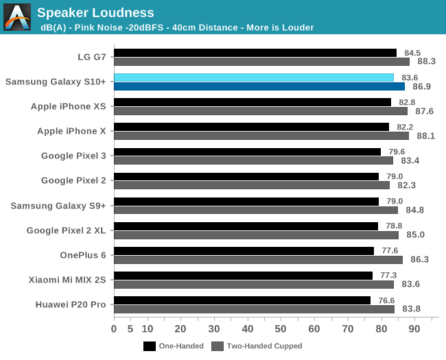
Looking at our speaker loudness tests, we see the Galaxy S10+ perform significantly better than the S9+. What is important to note here in the results is the very small difference in loudness between holding the phone one-handed in portrait mode versus holding it two-handed with cupped palms. The only other phones who had such small deltas were the Pixel 2 and Pixel 3’s front-facing speakers, however the Galaxy S10 goes a lot louder than both of these, without distortions if I might add. Currently the Galaxy S10 is the phone with the best frontal directionality in audio playback, something I did not expect.
Looking at the frequency response of the Galaxy S10, we see that Samsung not only makes the speakers loud, but they’re also of very high quality. The S10+ has notably improved the bass, upper-mid-ranges as well as treble versus the Galaxy S9+.
In fact the new upgrades on the S10 now put the phone comfortably ahead of any other smartphones in the market in terms of speaker quality, it’s just that much better.
The one thing I would critique Samsung on is the new volume control steps. The audio is now so loud and clear, that sometimes at night I want to have it set quieter, but the issue is that the new volume controls in OneUI have a lot less discrete steps, with less finer button-pressed levels than in previous generations, requiring one to fiddle with the volume slider to get to a certain volume. This is also valid for headphone playback.
3.5mm Headphone Jack Quick Note
Speaking of headphone playback, one thing I wanted to do late last year was reintroduce audio jack playback quality evaluation. This was something that was triggered by the loss of headphone jacks by many vendors who replaced them by low-quality 3.5mm dongles with bad audio quality. Only Apple unfortunately managed to deliver a sensible dongle with good audio quality.
During this testing I noticed that another difference between the Snapdragon and Exynos units is the audio quality of the DAC. The Exynos units have this reputation of being the ones with the high quality audio playback quality, but this is mostly just reputation based on these variants having Wolfon/Cirrus Logic audio chips, and not actual measurements.
Publishing audio measurements is like opening up Pandora’s box in terms of what I’m getting myself into, as very many people get it wrong. In many cases what you’re measuring isn’t actually the audio playback the audio device, but rather the input characteristics of your measurement hardware. Another popular mobile review site has as such been hitting the limits of their audio interface for several years now, with the resulting numbers not actually showcasing much of the capability of the devices at hand anymore.
As such, even my own figures here will be hitting the limits of my own measurement hardware, but if we keep in mind that these are not definitive measurements of the devices, then we can have a more balanced view. In particular for the Galaxy S10, these are very indicative of what you’re to expect as a difference between the two units.
Snapdragon Galaxy S10+
The Snapdragon Galaxy S10 continues to showcase excellent results with what was in line with Qualcomm’s Aqstic line of DACs over the last few years: a very clean output with very little noise.
Exynos Galaxy S10+
Switching over to the Exynos Galaxy S10 however we’re seeing some pretty shocking results. The phone uses a Cirrus Logic CS47L93 audio codec chip which has actually been used in Exynos variants since the Galaxy S7. Unfortunately in recent years this was surpassed by Qualcomm’s audio chips, and in particular the Galaxy S10 suffers from a pretty bad implementation. Here we’re clearly seeing noise components that are not part of the reference 1KHz signal, with a particularly odd 250Hz component. The measurements were done in sequence with just re-plugging the input from the Snapdragon to the Exynos under the same conditions. Audio output level was calibrated at near -10dbV / 312.5mV RMS on both devices.
In practical terms, there is audible difference between the two as the Exynos unit sounds warmer (in a bad way) and more muffled. The Snapdragon achieves higher clarity and the sound stage appears wider. This was my subjective evaluation using the same Samsung’s included AKG headphones on both units, both having the same software audio settings.
I applaud Samsung for still including the 3.5mm headphone jack on the Galaxy S10 – however a big part of the world will unfortunately experience lesser audio quality on their model variants.
As we’re wrapping up one of the biggest smartphone reviews to date, it’s also the wrap-up for one of the most important devices in 2019.
As early as last year I heard from some vendors that Samsung had big plans for the Galaxy S10, with the company aiming to make the device “something special” for its 10th year anniversary. While I believe Samsung has definitely raised the bar with the Galaxy S10, I'm left with mixed feelings on the phone overall. On the one hand it really is an almost perfect device, yet at the same time it also comes with many flaws.
The design of the new Galaxy S10 family, and in particular the S10+ is a stand-out feature of the new phones. In terms of aesthetics, the phone looks great with the new minimal bezels, however I think Samsung could have done better with the new cut-out camera designs. In particular, I would have liked to see the cut-out be slightly higher – placing it near the bezel of the screen – as to avoid having such a thick notification bar. Instead, this wasted space means that despite the larger screen and higher screen-to-bezel ratio, the top of the screen is no more useful on the Galaxy S10 than it is on the S9. Personally, I also didn’t like the visuals of the cut-out, however Night Mode in OneUI makes this a non-issue.
Another design change I didn’t care for was the new ergonomics: because the phone’s round edges now have a tighter radius, even though the absolute width of the S10+ hasn’t changed from the S9+, it actually feels like a bigger phone. The just released Huawei P30 Pro has almost the same width as the S10+, however those 1-2mm and the wider curve gradient with smaller bezel edges makes for a significantly more comfortable device. So if you’ve used the Plus variants of the S8 or S9 in the past, I’d actually recommend trying the regular S10 first. Finally, another oddity in the design of the S10+ is that the power button is just absurdly high up, which is a definite regression in ergonomics.
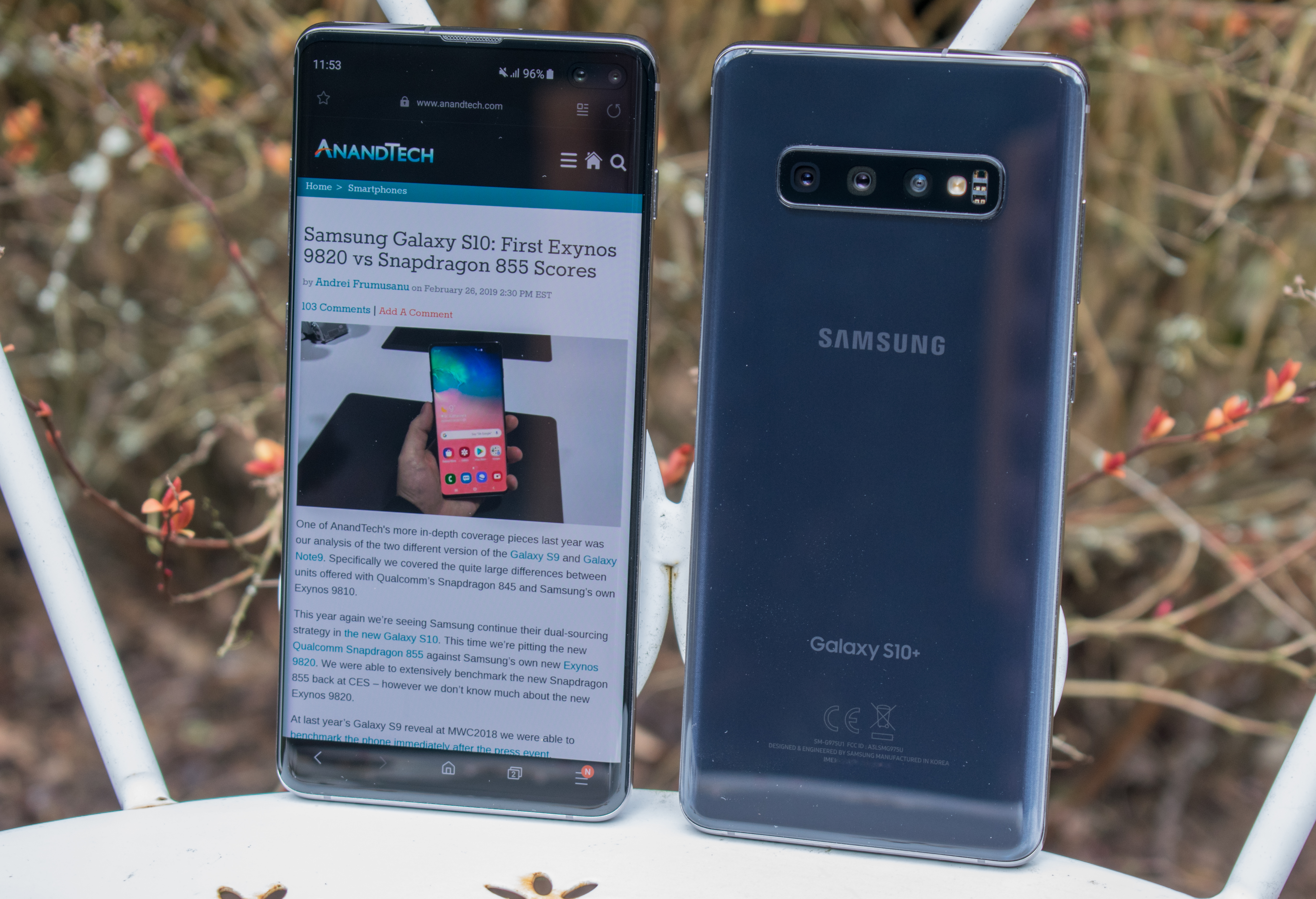
The screen of the Galaxy S10 is excellent, however there are still bugs in Samsung’s factory calibration. Getting correct gamma curves seems to be a major issue for Samsung, and we’re now in the Nth iteration of a Galaxy S phone where we’re seeing problems like this. The Exynos S10+ variant in natural mode has far too low and non-linear gamma, while the Snapdragon unit again clips the lower greyscale levels to black. This is fundamentally a software issue, and like in past years with the S8 and S9, Samsung will probably address it in a software update. I just wish Samsung would finally get their quality control to the point where they can get this correct for the phone's release, rather than having to fix the display settings after the fact. The screen for the third year in a row also has a too red default colour temperature.
In terms of display accuracy, Samsung does well, but it’s no Apple. Samsung’s choice of enabling Android’s colour management system on the S10 is weird. At least Samsung does have one first-party app supporting it: the Gallery, which is more than what you can say about Google's own Pixel phones. Beyond this, the inherent limitations of the Android CMS means that it’s nowhere near as useful as how it works on Windows or even the current gold-standard: Apple's iOS. I wish that Samsung would have at least enabled wide-colour gamut support for taking photos. Maybe that’s something for next year?
Two SoCs - This year more evenly matched
One of the bigger narratives for the Galaxy S series over the last few years were the product differences between the Snapdragon and Exynos units. 2018 in particular was a rough year for Samsung’s in-house developed Exynos variants, as the chip simply delivered a notably worse experience than what was available on Snapdragon 845 variants of the phones.
The Snapdragon 855 met our expectations and initial impressions of the new Qualcomm chip. The combination of Arm’s new Cortex-A76 CPU cores, Qualcomm’s Adreno GPU and DSP, and the new 7nm manufacturing node make for a fierce little chip. Power efficiency in particular is fantastic and the SoC represents be a solid foundation for many other flagships in the coming months.
Meanwhile the Exynos 9820 improves massively over its predecessor. This year, Samsung LSI has largely addressed some of the previous deal-breaking issues with the introduction of the new chip. On the microarchitecture side, the new Cheetah M4 cores don’t bring as big of an improvement as we would have wanted. Samsung’s IP still seems to lag behind the Cortex-A76, however the new cluster design and introduction of Cortex-A75 cores as the middle cores seems to have resolved the overall efficiency issues that the previous generation had.
In terms of performance, the Exynos chip slightly lags behind the Snapdragon, partly due to the microarchitecture differences, but mostly due to Qualcomm’s much more aggressive scheduler. With that said, in real-life daily usage (and thanks to better framework boosting mechanisms on the Exynos) the differences are actually minor. So you should have a harder time telling the difference between the two, with the end-result being a similar user experience.
The most surprising result in our testing was that both variants of the S10+ seem to be almost evenly matched in terms of battery life. The Exynos variant even has a slight advantage in our web test, while the Snapdragon variant pulls ahead in PCMark. It should be noted that the Exynos S10+ does suffer from some firmware issues at the moment which cause higher idle power consumption, however this fundamentally can be and should be fixed by Samsung in comfing updates, as it’s inherently not a hardware issue.
In absolute terms, both Galaxy S10+ models are now Samsung’s longest-lasting phones ever. Critically, Samsung seems to have taken hardware optimisations for battery life seriously, so the most important improvement for the S10+ isn’t its larger 4000/4100mAh battery, but rather the reduced base power consumption of the phone that is now 100-120mW below the Galaxy S9. This is the true reason the S10+ lasts so long. It’s fantastic to see Samsung focus on this aspect of battery life, and sets the new bar for the rest of 2019 for other vendors to meet.
Triple-cameras - surprising differences
Talking about cameras, the new wide-angle sensor on the Galaxy S10 is a fantastic addition, and it really augments the shooting experience. Currently it ranks as the best wide-angle shooter out there, battling with the Mate 20 Pro’s wide angle unit.
As for the rest of the camera modules, while the main camera and zoom module haven’t fundamentally changed much compared to the S9 in terms of specifications, the processing has changed dramatically. First of all, I applaud Samsung for keeping all three cameras for both the S10 and S10+ – no longer is the smaller version handicapped in the camera department.
The key new aspect of the S10’s cameras, beyond the wide angle module, is their far greater dynamic range, which looks to be significantly ahead of other phones. Samsung’s AI processing actually makes usage of the DSP and NPUs of the chipsets, and I think one of the results is that the Galaxy S10 now is now often spot-on in terms of exposure, colour-balance, as well as consistency between shots.


Snapdragon vs Exynos Galaxy S10+
One surprising revelation of our testing is that there are huge (and dare I say shocking) processing differences between the Snapdragon and Exynos S10+ variants. HDR on the Snapdragon unit is consistently superior, as it's able to achieve much better dynamic range and details in shadows. Furthermore, the Snapdragon unit’s colour rendition is more saturated and akin to the real-world, as opposed to the more washed-out pictures the Exynos variant produces. This difference is really accentuated on the wide-angle module shots. My Exynos unit’s wide angle camera suffered from inexplicable blurring off-centre, making me suspect that there are issues with the actual optics of that lens. If so, this is a quality assurance issue out of the factory as the module doesn’t even have an autofocus mechanism which might otherwise cause such an issue.
Low-light camera capture on the Galaxy S10+ is nothing special. Here the phones still largely lag behind Huawei’s capabilities, and the new Bright Night mode that the phone comes with is also no match against Huawei's Night Mode or Google’s Night Sight. I would have liked to see more usage of computational photography to improve the phone’s capabilities, especially given that the SoCs have the new IP blocks to enable it.
HDR10+ video recording is great, however it will be a pain to do anything with the resulting video files as there are big compatibility issues. Attempting to play back HDR recordings correctly on social media sites or any other non-HDR10+ device is a mess. Even Samsung’s software to convert videos to SDR is currently bad or just outright missing, something I hope will be addressed with coming software updates.
Finally, another difference between the Snapdragon and Exynos is the audio playback quality on the 3.5mm headphone jack. Unfortunately it looks like Samsung messed up with both the DAC as well as the implementation, as the Exynos Galaxy S10 has widened the existing year-long disadvantage to the Snapdragon.
Almost Perfect, Yet so Flawed
Overall, the Galaxy S10+ is an almost perfect device. At least, it would be if it weren’t for the fact that there's two of them. The Snapdragon Galaxy S10+ is actually the first phone I would have considered giving a gold award to, which considering that over the years I've never given an award to any phone should put things into context.
If you’re a reader in the US or other Snapdragon markets, you can stop reading here and feel happy about your purchase or go ahead and buy the Galaxy S10+.
Unfortunately the rest of the world gets another phone. Although battery life and performance this year aren’t an issue for the Exynos variant, the unexpected huge discrepancies in the camera quality, some screen calibration bugs, and the audio quality disparity all make this variant of the Galaxy S10+ a lesser choice. Except for the audio matter, most of these issues are software related. However I do have reservations if it’s even possible to make the camera processing equal to the Snapdragon.
Yet even with all these drawbacks, the Exynos variant of the Galaxy S10+ is still a great phone. It's just not as great as the Snapdragon version; which is to say that it's not as great as it could and should be. Consequently, interested buyers may want to wait a few months to get it at a cheaper price, making one feel better about the disadvantages it has against the Snapdragon.
Ultimately if Samsung wants to continue to compete against Apple and a surging Huawei in the ultra-high-end smartphone space, they will need to be able to deliver more consistent products across all markets. That Samsung Mobile division is not a vertically integrated with full control over their own silicon is now starting to show its disadvantages. It’s clear that vertical integration and more exclusive features is how things will go forward in the future for vendors who want to truly differentiate their products. In Samsung Mobile’s case, even with Samsung's incredible resources at their disposal, if they have to split their attention across two variants, it means each model will only get half the invested effort. Which, I suppose, is food for thought for what this means for the future of Samsung’s flagship devices.
https://www.anandtech.com/show/14072/the-samsung-galaxy-s10plus-review
2019-03-29 14:00:00Z
52780251840761
Tidak ada komentar:
Posting Komentar